

RISC processor implemented on an FPGA
2022 / Matías Bergerman, Agustín Galdeman, Franco Moriconi, Carola Pedrosa, Franco Scapolla
This project was made for the course 22.15 - Electronics V (Computer architecture), at the Buenos Aires Institute of Technology (ITBA).
Professors: Ing. Andrés Carlos Rodríguez, Ing. Pablo Enrique Wundes.
Base Design 🔗
Introduction 🔗
In this project, a RISC processor is implemented on an FPGA using Verilog. The hardware utilized is the Terasic DE0-Nano development platform, which features a Cyclone® IV FPGA.
The processor, named EV22 for “Electronics V 2022”, incorporates parallelism through a pipeline block and additionally includes a peripheral for video transmission via the VGA standard.
The base architecture design for the processor is as follows:
 EV22 architecture.
The EV22 processor is a RISC processor with 16-bit registers and buses. Its opcodes are 14 bits, and it includes an 8-bit constant register. The instruction set contains 27 instructions, with each instruction corresponding to a single microinstruction.
Arithmetic operations are performed through an ALU with two 16-bit inputs and one 16-bit output. The inputs are labeled A and B, and the output is Z, but it is renamed as the C Bus at the shifter’s output. Input A is the output of a multiplexer, whose inputs are either a register from the Register Bank or the value in the constant register. The “ALUC” bits determine the arithmetic operation the ALU performs in each microinstruction. Input B can only take values from registers within the Register Bank. The ALU has a Carry Block to store a carry bit if necessary during an operation, but it can also be explicitly configured through instructions.
The program memory is read-only, separate from the read/write memory where data is stored, making this a Harvard architecture.
The processor features a Register Bank with 35 registers. Of these, 28 are general-purpose, 2 are associated with input pins, another 2 with output pins, 2 are internal to the Register Bank for auxiliary use and are not directly accessible to the program, and there is 1 register called the Working Register. The programmer uses the Working Register to read values from memory or other registers and perform calculations with them. Logically, it is simply another register, but most instructions operate explicitly and directly with this register.
Execution Flow 🔗
The first column of the following figure shows the opcodes for each instruction on the EV22:
 Original instruction set.
It is noteworthy that most of them have variable fields denoted by the letters “i”, “j”, “k”, “y”, “x” and “s”. In these sections of the opcodes symbolized by letters, some numerical value is entered that the instruction itself will use in its operation. For example, “JMP X” is an unconditional jump identified by the value “100” which uniquely defines the opcode and then the next 11 bits indicate to which position the Program Counter will jump.
Having established the format of the instructions, the execution flow in this reference implementation is, in general terms, as follows:
- The Program Counter tells the memory named “Program” which memory location to access.
- The Instruction Register interprets the memory location read and propagates its contents.
- The Micro-instruction ROM decodes the instruction into micro-instructions and propagates to the pipeline.
- The ALUC, SG, KMx, etc. fields take values depending on the opcode to set the constants register, A and B latches, ALU operation, etc.
- The ALU performs some operation, except for jump instructions.
- The output of the ALU is stored in some Register Bank register or used to store information in the RAM called “DATA”.
The main exception to this flow are jump instructions, which are determined through “Block 1” which makes direct use of the first bits of the BUS from which the instruction is retrieved, in conjunction with combinational logic, and takes inputs such as Carry or the value of the Working Register, which are used to determine whether a jump should be made or not.
Implementation of the EV22-G3 🔗
Instruction Set 🔗
Our practical implementation, called EV22-G3, is strongly based on the scheme proposed in the previous section. However, it has some differences. Mainly, the instruction set was modified with two additional bits per instruction, generating 16-bit opcodes instead of 14 in order to use a more common word length and at the same time adding the necessary functionality to support 16-bit constants and registers. The following table shows the EV22-G3 instruction set.
 EV22-G3 instruction set.
The main differences are:
- The opcodes have two additional bits and are now 16 bits.
- It incorporates the NOP instruction, which does not exist in the original design.
- It incorporates the LSK instruction, which is used to define the least significant byte of the constant.
- The opcode 0x0000 is used for NOP instead of Complement Working Register.
- The opcodes ANR, ADR, CLR and RET were modified so that B7 is 0 and B14 is 1. This simplifies the combinational logic of the decoder.
- It incorporates the PIX RGB and PIX W instructions to support the VGA video peripheral.
With the LSK instruction, the K constant register can become a 16-bit register, which is loaded with a value in two steps: First, the least significant byte is loaded with LSK without performing any other operation. Then, a second instruction will load the MSB and at the same time perform some action, such as saving the contents of the K register to the Working Register or performing some operation on the register contents.
Registers R26 and R27, in addition to being used as general purpose registers, play a role in controlling the VGA peripheral. When executing the PIX RGB instruction where a color value is set as a literal constant, or PIX W where the color value corresponds to the last 3 bits of the W register, the VGA peripheral modifies the color of the pixel in row R26 and column R27 of its internal RAM to write the color value indicated.
Adding two additional bits to each opcode takes advantage of the 16-bit processor buses and registers. These additional bits are used to decode the different opcodes more efficiently.
Logical implementation on the Intel® Quartus® Prime Software 🔗
Translating the blocks from the original architecture diagram into an implementation on the Quartus software is not straightforward. Nevertheless, for practical purposes, the functions and original roles of these blocks are maintained.
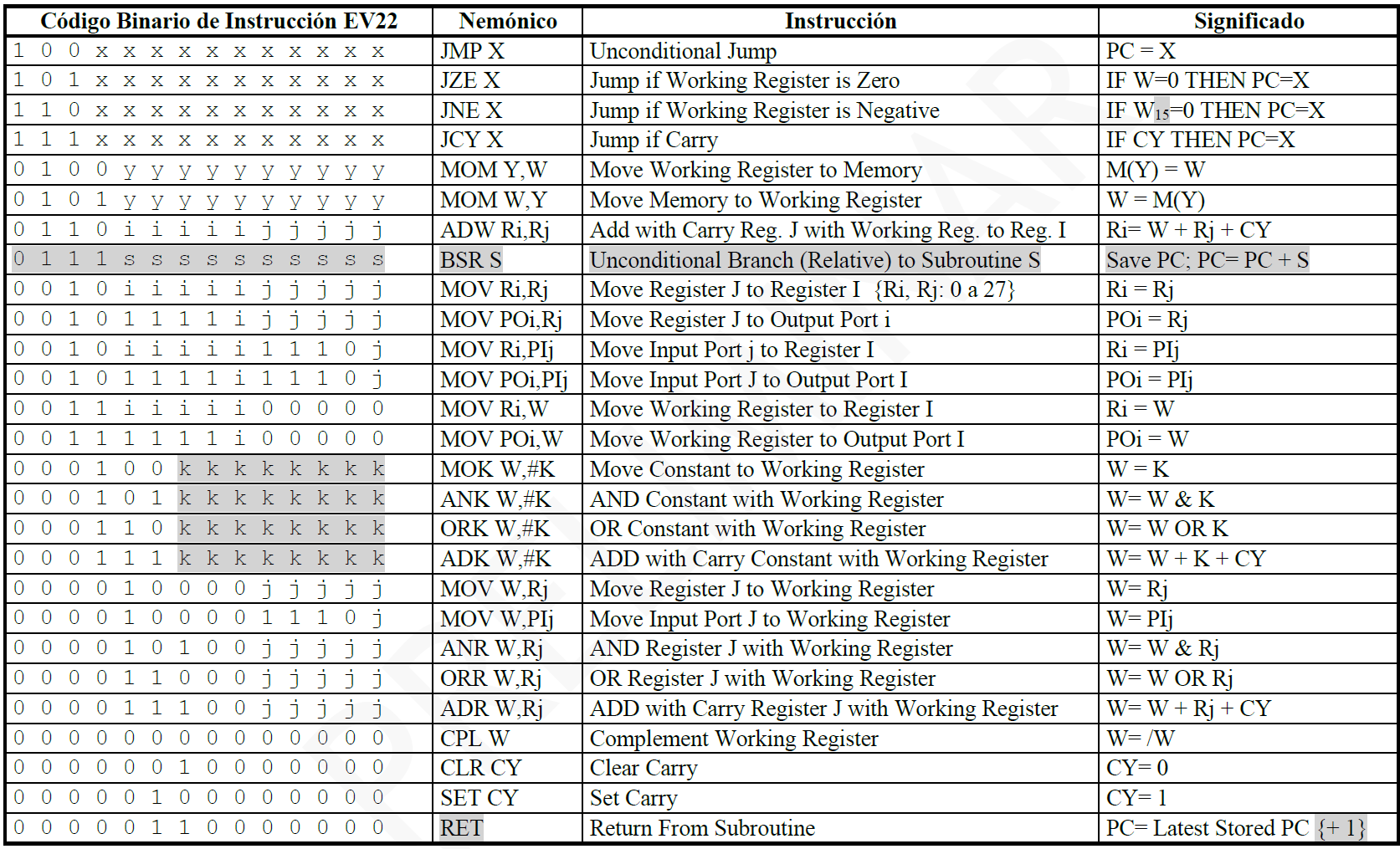
Fetch Unit 🔗
To analyze the HDL implementation, we start from the beginning of the program flow. A Fetch Unit was implemented with a clock input and a counter that performs the role of the Program Counter register, and is the blocks only output. This fetch unit contains logic that will modify the program counter if any instruction demands it, such as jumps or subroutine calls/returns.
 Fetch Unit and Block 1.
The Fetch Unit inputs are:
- clk_pc: Clock that feeds into the block and increments the counter.
- nReset: Reset button. It has an associated physical input.
- Type: Takes the “type” output of the current microinstruction as a condition to make decisions.
- B1_OUT: It takes the output of a bit from Block 1 that indicates if a jump must be made.
- Opcode: Uses some bits of the current opcode to make decisions.
- SR_OUT: It is used to make decisions regarding subroutine calls and returns.
Next there is Block 1, which works in a very similar way to the original scheme presented. Its inputs are:
- OPCODE: It uses bits of the opcode to make decisions.
- CY_OUT: It is used to decide whether to jump in the JCY X instruction.
- WR: Used to decide whether to jump depending on whether it is zero or negative for the JZE X and JNE X instructions respectively.
Its outputs are:
- B1_OUT: Tells the Fetch Unit whether to modify the PC because the conditions for a jump are met.
- SR_OUT: Tells the Fetch Unit if it must modify the PC because it is returning from a subroutine.
Between these two blocks, the program flow is controlled. The program counter addresses a ROM where the program to be executed is stored.
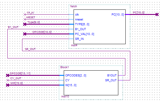
ROM 🔗
 ROM where the program is stored.
The ROM is simply a memory addressed by the PC, which indicates the position to read from memory and send its contents to the output. A clock feeds a latch that allows the PC address to reach the ROM. The output has no latch since the new OPCODE needs to be output immediately for the next stage of an instruction cycle.
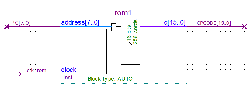
Decoder 🔗
 Decoder.
The Decoder block includes the modules interpreting instructions and microinstructions. Its only input is the opcode obtained from the ROM which is addressed by the PC. It uses a switch-case with the opcode value that, depending on the opcode, returns the values of ALUC, SH, KMux, MR, MW, etc. according to the instruction set. Thus, it translates the opcode and configures the rest of the processor to perform the task specified in the opcode, indicating the ALU operation type, which input registers to use, which RAM address to use, whether it is a read or write operation, etc.
Constant Register 🔗
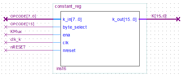 Constant Register.
This register receives, from certain opcodes, 8-bit values that it will store in its most-significant or least-significant byte as appropriate and thus form a 16-bit word that will then feed the input A of the ALU. However, its output first passes through a MUX which will then choose whether A should receive the value from this register or from some Register Bank register.
Among its inputs, it has:
- OPCODE[7..0]: If the instruction involves loading values to this register, that value is in these bits of the opcode.
- OPCODE[15]: If the current instruction modifies the register in any way, the most significant bit is the one that indicates whether the 8 bits are loaded into the LSB (if it is 0) or the MSB (if it is 1).
- KMUX: It comes from the Decoder. If it is 1, this register will use the previous entries to load a new value. If it is 0, it does nothing.
- clk: It is the clock that feeds the register and is synchronized in such a way that it only acts after the PC is updated and the new opcode is already available.
- nRESET: If the reset is activated, this register is cleared and becomes 0 by default.
Arithmetic logic unit (ALU) 🔗
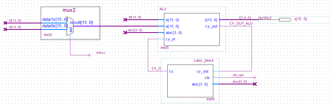 Arithmetic logic unit (ALU).
The ALU works in the same way as in the original architecture proposal. Its inputs are A and B, the output is Z, and there is a CY input coming from the carry block which in turn receives the ALU output. No shifter is incorporated since no operation in the instruction set uses one, but it could be incorporated without major changes. The ALU is not clocked, all its operations occur as soon as any parameter changes at its input. As mentioned before, A comes from a MUX that selects which value to read, B comes exclusively from the Register Bank and Z (or C) goes directly to the Register Bank.
The Carry Block updates the carry only when ALUC indicates that the ALU is performing an operation that modifies the carry, including set carry and clear carry.
Register Bank 🔗
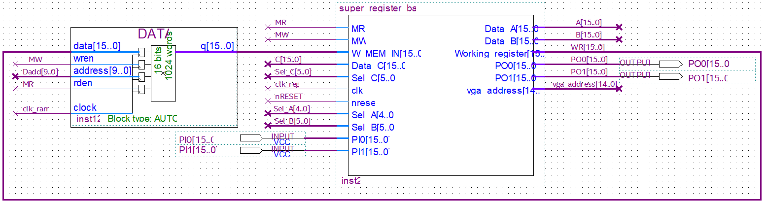 Register Bank and Data.
The figure shows the Register Bank block and the RAM where data is stored if an opcode indicates it. The Register Bank is split into multiple sub-stages. The original diagram proposed by the professors is shown to explain what the implementation is based on.
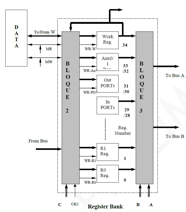 Register Bank original design.
Internally, the Register Bank is separated into three parts:
- Block 2: It communicates with the RAM bidirectionally using MR and MW. It also receives the output of the ALU, a clock and a value (called C in the figure) that indicates in which register to store the contents of the C bus. Its output is the C bus value at the address indicated by the corresponding input.
- Block 3: It communicates with buses A and B to perform ALU operations. Its inputs are the values of the registers, and which registers to read for A and for B. It has no clock.
- Registers: All the registers explained in the first section. The output of the Working Register is used for Block 1 logic and goes to Block 2 to store the contents in memory, or load it, as appropriate.
In the practical implementation, Block 2 and the register area are not separate. Both sections were incorporated into a single block within a Verilog “always” block. Separating them explicitly resulted in an additional layer of complexity that did not provide any advantages and led to synchronization problems in Verilog.
Block 3 is essentially just two multiplexers whose input are all the registers (except the output pins), so it was kept separate from Block 2 and the register space. It was implemented as a verilog function, so that when an opcode changes the values of the registers to be read in A and B, it instantly updates the ALU with the new value.
The Register Banks entries are:
- MR: Indicates a read from RAM
- MW: Indicates a write to RAM
- W MEM IN: Value read from the RAM.
- Data_C: Output from the ALU, via the C bus.
- Sel_C: Comes from the Decoder. It indicates where to save the content of the C bus.
- clk: The clock that feeds the logic corresponding to the functions of Block 2.
- nRESET: Reset. If activated, all registers return to zero.
- Sel_A: Comes from the Decoder. Indicates which register should read input A of the ALU.
- Sel_B: Comes from the Decoder. Indicates which register should read input A of the ALU.
- PI0: Input port 0
- PI1: Input port 1
The RAM receives MR and MW that tell it whether a write or read operation is being performed. Dadd, coming from the decoder, indicates which memory address to read, in the same way that PC did with the program ROM. It has a “Data” input for write operations that comes from the output of the Working Register since this register mediates between the common registers and RAM, and it has a “q” output which is used in read operations.
Pipeline 🔗
Pipeline Stages 🔗
The scheme followed for the the pipeline separation into different stages was very similar to the one proposed by the professors, with the differences in the decoder block mentioned above. The decoder block is a combination of the decode and operand stages, followed by the execute and retire stages. In addition, another change that was proposed is to implement the UC1 block as a purely combinational block.
UC1 Block 🔗
The UC1 block is in charge of inserting NOPs in the pipeline in cases where the Hold conditions are met. For this, it is only necessary to set the value of C to 35 so that the result is not saved, and to insert zeros in the “type” field. In addition, it must be possible to propagate the memory read or write signals to the rest of the pipeline.
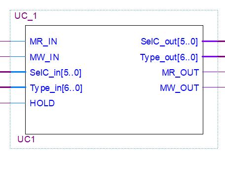 UC1 Block.
Conflict resolution: UC2 Block 🔗
Another fundamental block for the operation of the processor is the UC2 block, which is in charge of resolving the dependencies between instructions, and in case of finding conflicts between them, it triggers the Hold signal to wait for the pipeline to be emptied and thus avoid errors in the programs. To evaluate if there are conflicts between instructions, the signals Type2, Type3, Type4 and Type5, SelA2, SelB2, SelC3, SelC4 and SelC5 are received. The Type signals reference which registers are written and read by each instruction. The order and naming for each bit used was as follows:
\(T_i\) corresponds to the i-th Type signal, b is each bit with its subscripts representing the interaction with each register (J for the PC, R for general purpose registers and W for the working register).
Using this scheme it is possible to identify 4 types of conflicts:
- That the Working Register is to be read when stage 3, 4 or 5 wants to write to it.
- That the carry is to be used when stage 3, 4 or 5 wants to write to it.
- Conflicts in cases where there are jumps.
- Conflicts in the general-use registers, it must be avoided that the lower stages of the pipeline write to them while the higher stages want to read them at the same time.
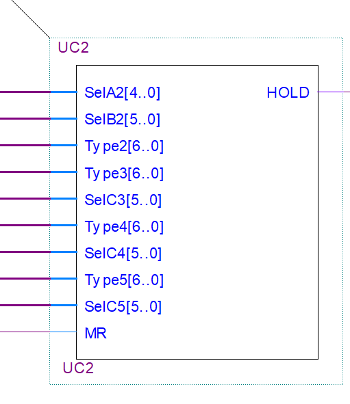 UC2 Block.
Pipeline registers 🔗
The rest of the pipeline is composed of two registers: MIR2 and MIR3. These registers propagate the signals corresponding to the following stages and to the processor modules that require them. Each one receives its clock with the necessary offset to allow for a correct propagation.
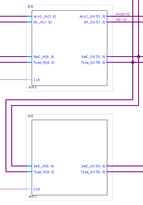 Pipeline.
Custom improvement: VGA peripheral 🔗
Aside from the basic EV22 scheme, an additional RAM was incorporated. This RAM uses two clocks. One at the input, to operate the VGA RAM in the same way as the program ROM and the Data RAM, and a second clock at the output whose frequency is dictated by the screen to be used, since the output of this memory is physically written to pins of the FPGA, which connect to monitor VGA port.
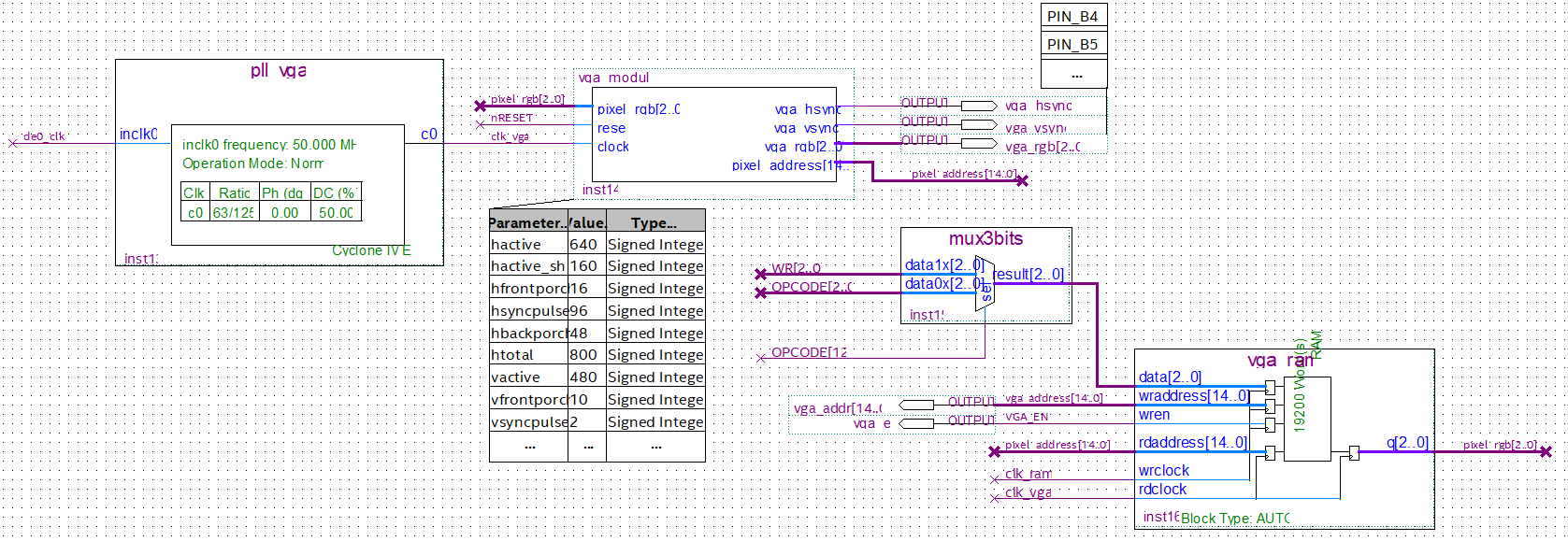 VGA Logic.
Only eight colors are available, as each pixel is represented by three bits. The resolution is not particularly high, as a consequence of the memory available on the FPGA. However, arbitrary images that were used as examples managed to be reproduced relatively clearly despite the hardware limitations. Real-time image manipulation tests were performed, which functioned without major problems.
The RAM memory can be initialized using a Memory Initialization File (MIF), which is generated from a JPEG image using a Python program1.
Simulations 🔗
To create codes in Assembly for the simulations, as well as to perform tests on the FPGA, a simple Python compiler was implemented that automatically translates the abbreviations of each opcode into the corresponding bitfile to be uploaded on the FPGA using the HEX format (Intel hexadecimal object file format).
Functional simulation with no pipeline 🔗
The following figure shows a simulation run in Quartus with a simple code that generates a Fibonacci sequence:
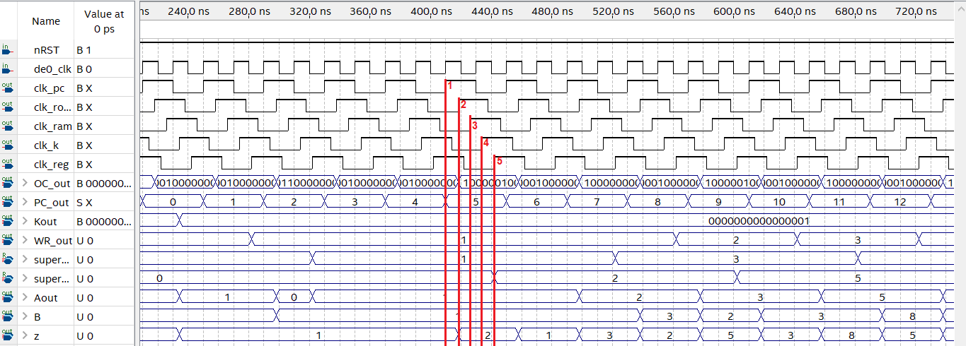 Timing diagram on a standard program.
Assembly code that generates the Fibonacci sequence::
LSK #K      1       // K_lsb = 1
MOK W,#K    0       // K_msb = 0; Wr = K
MOV Ri,W    0       // Move Wr to R0

LSK #K      1       // K_lsb = 1
MOK W,#K    0       // K_msb = 0; Wr = K

// Repeat the next 4 instructions forever:
ADW Ri,Rj   1 0     // R1 = Wr+R0
MOV W,Rj    0       // Wr = R0
ADW Ri,Rj   0 1     // R0 = Wr+R1
MOV W,Rj    1       // Wr = R1
...
The figure shows five red lines, which are the phase-offset clocks with the value changes in the different stages of the program flow. The order proposed and used for the correct operation of the processor was as follows:
- Program Counter
- Latch ROM input
- Latch RAM input
- Register Constants (K)
- Register Bank
This enumeration corresponds to the one shown in the simulation figure. First, the Program Counter is increased, which results in an opcode change. In this case, no information is accessed in RAM so the clock named “clk_ram” does not change. Then, when a cycle of the Constant Register clock starts, it is updated to the value that was loaded through the corresponding opcode, although in this particular case the Fibonacci code only needs it to be done once at the beginning of the program to initialize the sequence, so this change is not aligned with line 4. Finally, the Register Bank is updated by storing or reading some register as requested. The figure shows how the result of the calculation in the ALU (Z) is stored in one of the registers.
The PLL used operates at 50MHz, but the processor operates at 25MHz. This value was chosen because of the limitations of the digital analyzer used to measure the implementation of the processor in a real FPGA. The analyzer used was the Digilent Electronics Explorer, whose bandwidth limitations when sampling start to become noticeable at frequencies higher than 25MHz. The Quartus timing simulation suggests that there should be no problem in using higher frequencies, such as two or four times the 50MHz that are fed to the PLL, but since it was impossible to verify this in practice, it was decided that the safest way was to use a frequency where the correct operation of the FPGA with the processor loaded could be confirmed.
Tests 🔗
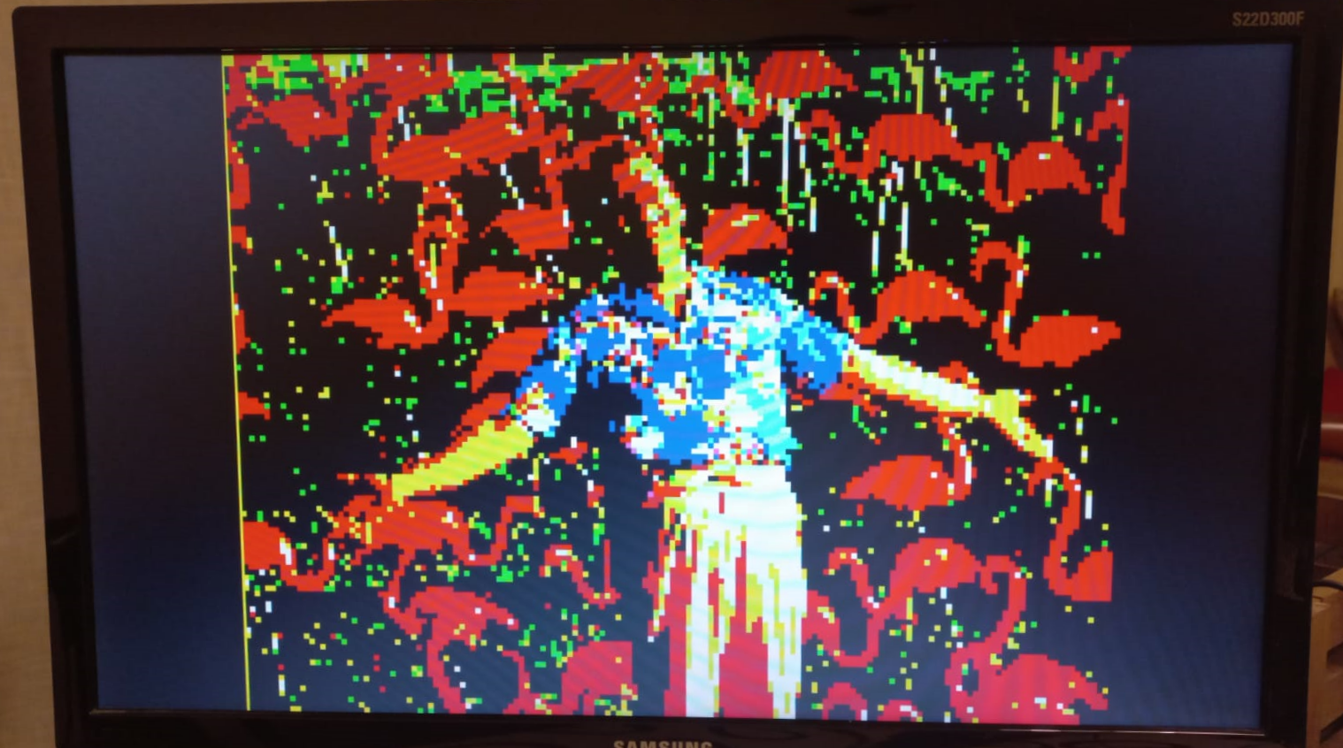
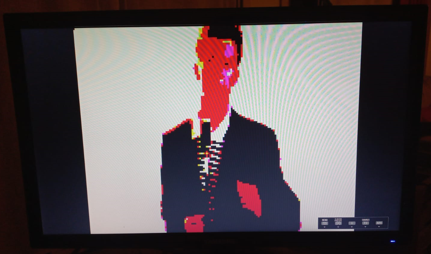
The EV22-G3 was programmed on the Cyclone IV FPGA present on the evaluation board DE0-Nano. A VGA monitor was connected to the board using some passive components to adapt the voltage levels.
In the figures below two examples are shown of images that were pre-loaded into the memory of the VGA peripheral, along with a picture of the monitor when connected to the FPGA. The resolution of the image produced is 120x160 to use less memory, but this can be easily increased by adding more memory to the FPGA. However, to achieve a number of colors greater than 8 a DAC should be added that can produce the analog values corresponding to each color.
Picture of Don Featherstone: Original, and recreation on a monitor by the EV22-G3.

Picture of Rick Astley: Original, and recreation on a monitor by the EV22-G3.

Finally, as an example, an Assembly code is shown that goes pixel by pixel through the RAM memory of the VGA peripheral and paints the whole screen blue, except for a 16x16 rectangle that is painted red. By modifying the value of 4 general purpose registers it is possible to draw the rectangle at any position on the screen, and the VGA peripheral will update the image.
LSK #K      B0      // Cargo el indice X            // K_lsb = B0
MOK W,#K    FF                                      // K_msb = FF; Wr = -80
MOV Ri,W    03                                      // Mover Wr a R3
LSK #K      C4      // Cargo el indice Y            // K_lsb = C4
MOK W,#K    FF                                      // K_msb = FF; Wr = -60
MOV Ri,W    04                                      // Mover Wr a R4
LSK #K      00      // Cargo el contador de colores // K_lsb = 00
MOK W,#K    00                                      // K_msb = 00; Wr = 00
MOV Ri,W    02                                      // Mover Wr a R2
LSK #K      00      // Cargo el contador de colores // K_lsb = 00
MOK W,#K    00                                      // K_msb = 00; Wr = 00
MOV Ri,W    02                                      // Mover Wr a R2
LSK #K      88      // Cargo el contador de filas   // K_lsb = 88
MOK W,#K    FF                                      // K_msb = FF; Wr = -120
MOV Ri,W    0                                       // Mover Wr a R0
LSK #K      00      // Cargo el valor de fila       // K_lsb = 00
MOK W,#K    00                                      // K_msb = 00; Wr = K
MOV Ri,W    1A                                      // Mover Wr a R26
LSK #K      60      // Cargo el contador de cols    // K_lsb = 60
MOK W,#K    FF                                      // K_msb = FF; Wr = -160
MOV Ri,W    1                                       // Mover Wr a R1
LSK #K      00      // Cargo el valor de columna    // K_lsb = 00
MOK W,#K    00                                      // K_msb = 00; Wr = K
MOV Ri,W    1B                                      // Mover Wr a R27
MOV W,Rj    03      // Traigo el indice X           // Wr = R3
ADR W,Rj    1B                                      // W = W + R27
JNE X       29      // Comparo R27 con el indice X  // No pintar (jmp 41)
LSK #K      F0      // Cargo el -ancho X            // K_lsb = F0
MOK W,#K    FF                                      // K_msb = FF; Wr = -16px
ADR W,Rj    03                                      // W = W + R3
ADR W,Rj    1B                                      // W = W + R27
JNE X       21      // Comparo R27 con X+width      // Pintar (Check Y)
JMP X       29      // Pinto color de fondo         // No pintar (jmp 41)
MOV W,Rj    04      // Traigo el indice Y           // Wr = R4
ADR W,Rj    1A                                      // W = W + R26
JNE X       29      // Comparo R26 con el indice Y  // No pintar (jmp 41)
LSK #K      F0      // Cargo el -alto Y             // K_lsb = F0
MOK W,#K    FF                                      // K_msb = FF; Wr = -16px
ADR W,Rj    04                                      // W = W + R4
ADR W,Rj    1A                                      // W = W + R26
JNE X       2B      // Comparo R26 con Y+height     // Pintar (jmp 43)
PIX RGB     01      // Pinto de color Azul (fondo)
JMP X       2C      // Continuo, avanzo PC en 2
PIX RGB     04      // Pinto de color Rojo (rectangulo)
LSK #K      1                                       // K_lsb = 1
MOK W,#K    0                                       // K_msb = 0; Wr = K
ADW Ri,Rj   1B 1B                                   // R27 = Wr+R27
ADW Ri,Rj   01 01                                   // R1 = Wr+R1
MOV W,Rj    01                                      // Wr = R1
JZE X       33      // Me salteo el JMP X
JMP X       18      // Vuelvo a ejecutar PIX RGB
LSK #K      1                                       // K_lsb = 1
MOK W,#K    0                                       // K_msb = 0; Wr = K
ADW Ri,Rj   1A 1A                                   // R26 = Wr+R26
ADW Ri,Rj   00 00                                   // R0 = Wr+R0
MOV W,Rj    00                                      // Wr = R0
JZE X       C      // Termina la imagen
JMP X       12     // Reinicio las columnas