

Design of a Flyback power supply
2022 / Matías Bergerman, Franco Moriconi, Carola Pedrosa, Franco Scapolla
Design of the power supply 🔗
The objective of this work is to design a Flyback power supply with an input of $220\ V_{AC_{RMS}}$ and an output of $12\ V_{DC}$. This design uses a feedback circuit with an optocoupler and the TNY290PG1 integrated circuit. According to the characteristics of the IC, a target output power of $30W$ was determined.
To begin with, we started with the typical application circuit provided by the manufacturer, which can be seen below:
 Typical application circuit provided by the manufacturer.
Starting from this circuit, a voltage rectifier is added to the input, a resistor to detect the under-voltage between the line and the EN/UV pin of the TNY290PG, and a variable resistor in series with the optocoupler LED to allow for a fine adjustment of the output voltage. Additionally, a resistor is added in series with the transformer primary coil to perform current measurements, as well as various voltage measurement pins. The BP capacitor is selected according to the desired current limiting, and the snubber circuit is designed according to the Fairchild Semiconductors application note number AN41472. The only modification that is made to it is the addition of a 100 ohm resistor in series with the snubber diode in order to attenuate the resonance of the circuit between the snubber capacitor and the transformer inductances at the moment of switching. The final circuit can be seen below:
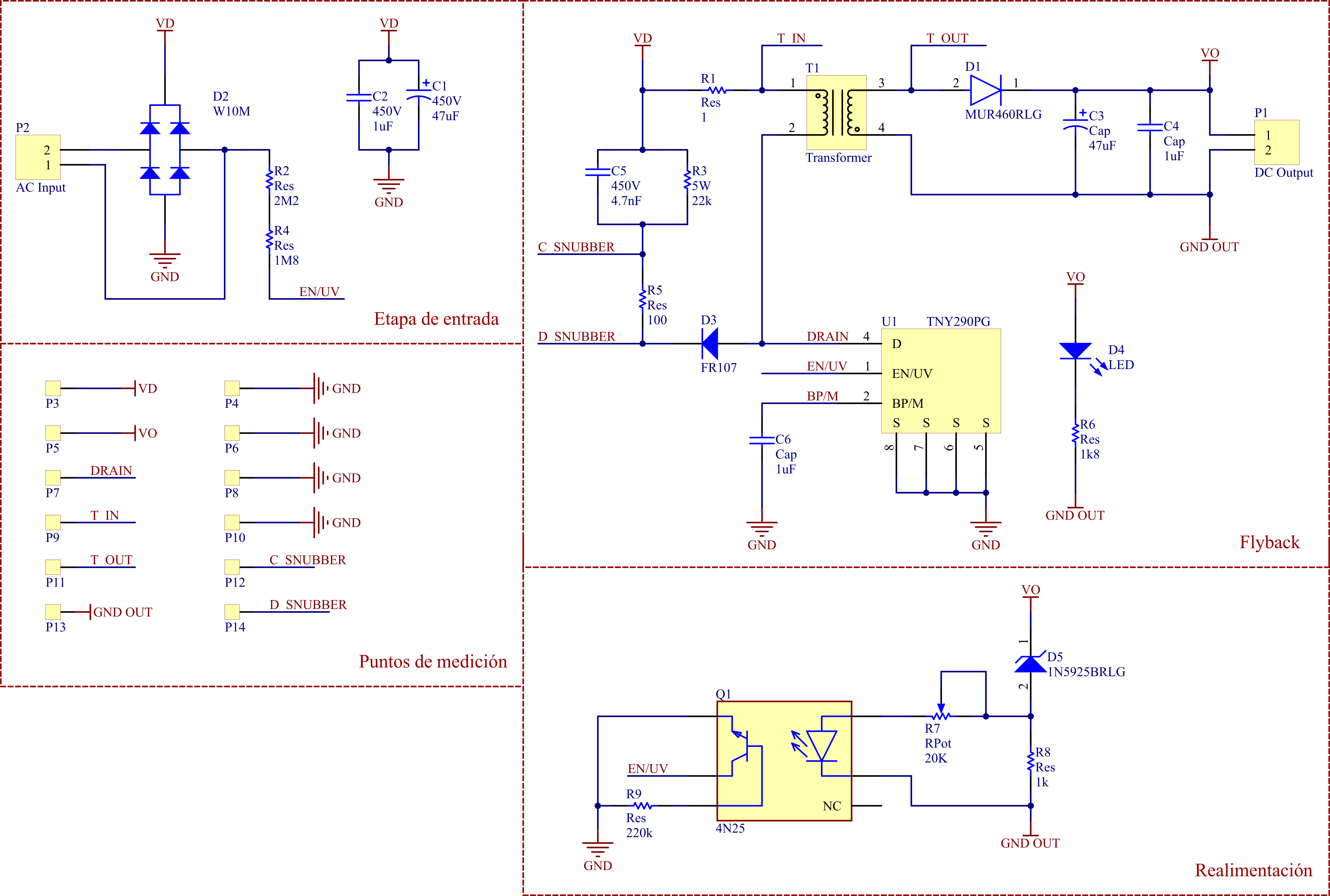 Circuit design.
To implement this circuit on a PCB, the indications given by the manufacturer of the TinySwitch integrated were followed:
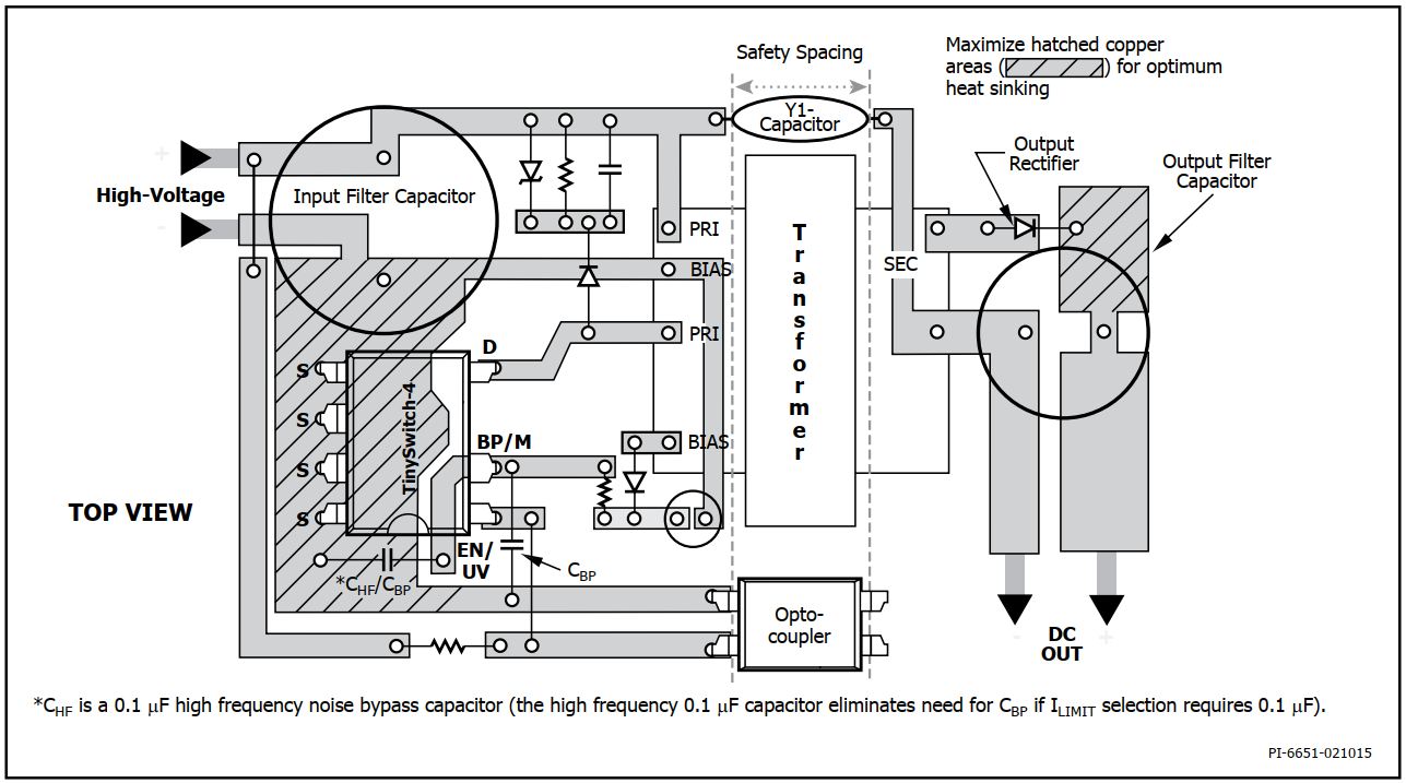 Manufacturer design recommendations.
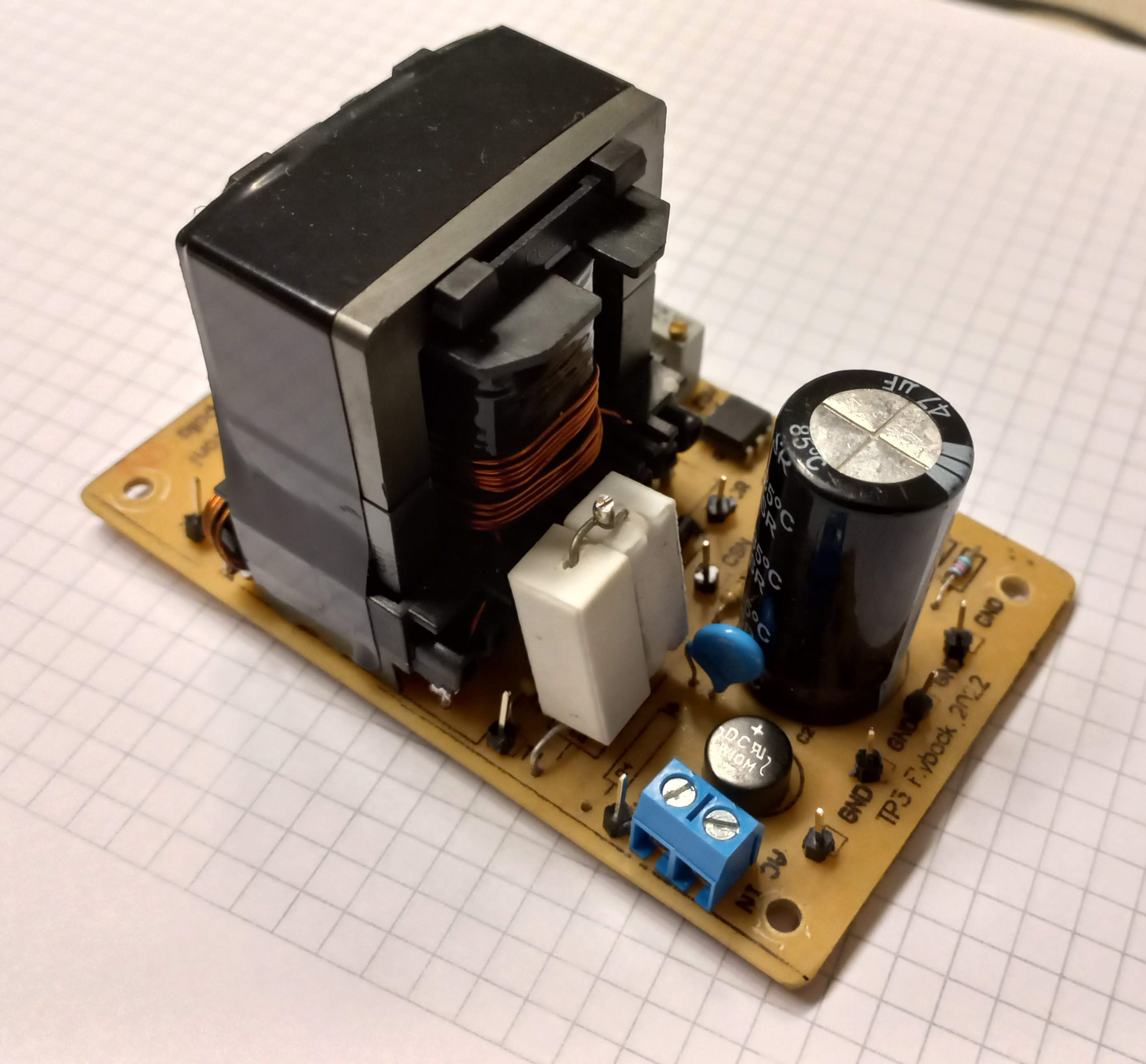
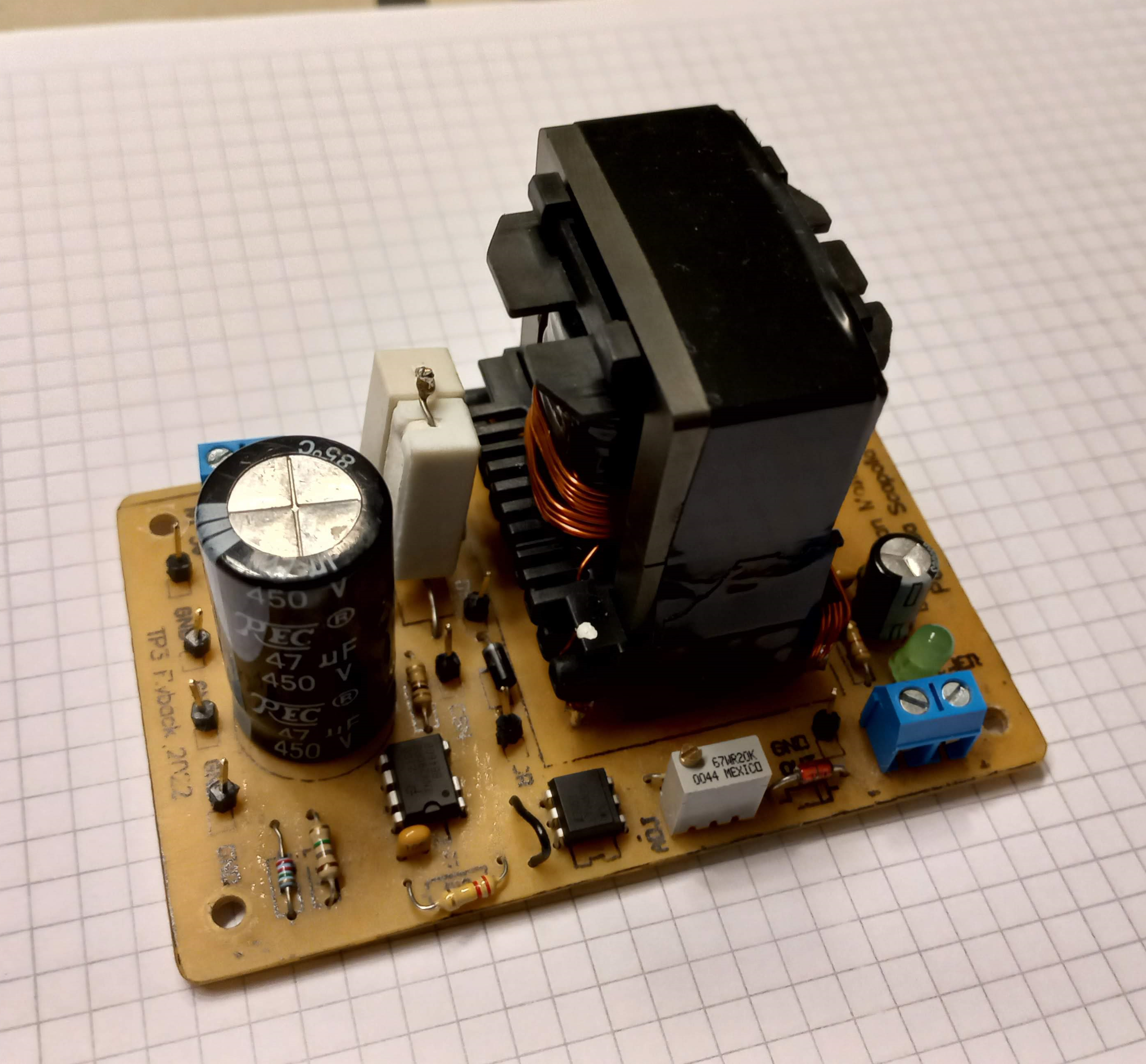
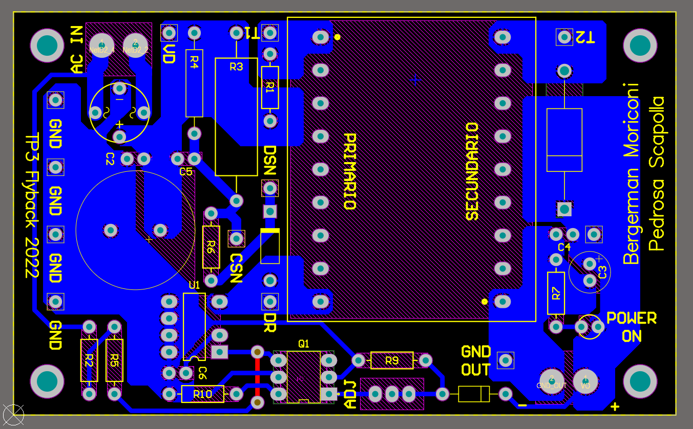
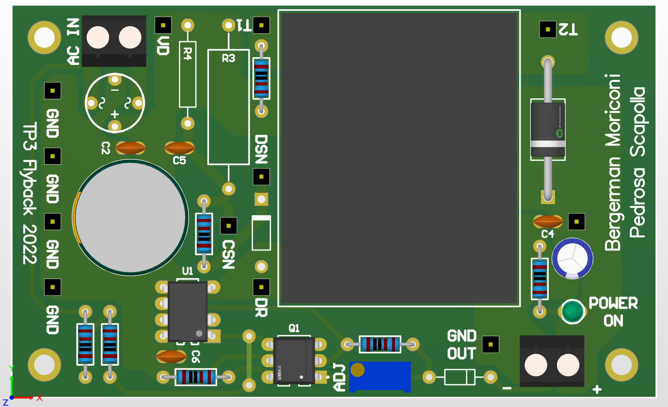
An image of the designed PCB can be seen below:
The main design parameters can be seen in the Table below. Some of these parameters had to be slightly modified according to the availability of components.
| Parameter | Value | Unit |
| Output Power ($P_o$) | 30 | W |
| Output Voltage ($V_o$) | 12 | V |
| Input Voltage ($V_i$) | 311 | V |
| Typical Duty-Cycle | 0,4 | |
| Switching frequency ($f_s$) | 132 | kHz |
| Primary inductance ($L_1$) | 5 | mHy |
| TinySwitch-4 $I_{LIMIT}$ | 0,75 | A |
| Core $A_L$ | 5200 | nHy/N² |
| Current Density ($J$) | 3 | A/mm² |
| Primary effective area | 76,8 | mm² |
| Secondary effective area | 76,8 | mm² |
| $B_{sat}$ | 200 | mT |
| Core $A_{min}$ | 229 | mm² |
| Available wire radius ($r_2$) | 0,3 | mm |
| Output voltage ripple | 1 | % |
| Switch breakdown voltage | 725 | V |
| Measured leakage inductance | 177,3 | uHy |
| $C_{SN}$ voltage ripple | 7,3 | % |
From the design parameters, the rest of the parameters necessary to carry out an implementation of the circuit were calculated. The results and the components selected to suit them can be seen in the following Tables:
| Component | Value |
| Output diode | MUR460 |
| Output capacitor | 47uF |
| BP capacitor | 1uF |
| Full bridge rectifier | W10M |
| Input capacitor | 47uF |
| Optocoupler | 4N25 |
| Zenner diode | 10V |
| Variable resistor | 20 kOhm |
| $R_{SN}$ | 22 kOhm |
| $R_{SN}$ power | 5 W |
| $C_{SN}$ | 4,7 nF |
| Snubber diode | FR107 |
| Parameter | Equation | Value | Unit |
| Average output current | $P_o/V_o$ | 2,5 | A |
| Transformer turn relation ($N_1/N_2$) | $1/\left(\frac{V_o}{V_i}\cdot\frac{(1-D)}{D}\right)$ | 17,2778 | |
| Output current measured during switch turn-off ($I_{X_2}$) | $I_{o_{avg}}/(1-D)$ | 4,1667 | A |
| Output current measured during switch turn-on ($I_{X_1}$) | $I_{X_2}\cdot\frac{N_2}{N_1}$ | 241,2 | mA |
| Average input current ($I_{i_{avg}}$) | $I_{X_1}\cdot D$ | 96,5 | mA |
| Input power | $V_o\cdot I_{i_{avg}}$ | 30 | W |
| Peak input current ($\hat{I_i}$) | $I_{X_1}+(D\cdot T_s/2\cdot V_i/L_1)$ | 335,4 | mA |
| Number of turns for the primary side ($N_1$) | $\sqrt{L_1/A_L}$ | 31 | |
| Number of turns for the secondary side ($N_2$) | $N_1 / \frac{N_1}{N_2}$ | 1,8 | |
| Skin depth ($d$) | $66/\sqrt{f_s}$ | 0,1817 | mm |
| Primary wire minimum radius ($r_1$) | $\frac{I_{i_{avg}}/J+d^2\cdot\pi}{2\cdot d\cdot\pi}$ | 0,1190 | mm |
| Inductance of the secondary side ($L_2$) | $\frac{N_1/N_2}{ {L_1}^2 }$ | 16,7 | uHy |
| Secondary peak current ($\hat{I_2}$) | $\hat{I_i}\cdot \frac{N_1}{N_2}$ | 5,79 | A |
| Secondary minimum current ($I_{2_{min}}$) | $2\cdot I_{X_2} - \hat{I_2}$ | 2,54 | A |
| Output RMS current ($I_{o_{RMS}}$) | $\sqrt{(1-D)/3\cdot(\hat{I_2}^2+\hat{I_2}\cdot I_{2_{min}} + {I_{2_{min}}}^2)}$ | 3,31 | A |
| Minimum number of turns for the secondary | $\frac{I_{o_{RMS}}}{(r_2^2\cdot\pi-{(r_2-d)}^2\cdot\pi)\cdot J}$ | 4,6194 | |
| $V_{switch}$ | $V_i + V_o \cdot \frac{N_1}{N_2}$ | 518,33 | V |
Circuit simulation 🔗
Due to the lack of an appropriate SPICE model to simulate the behavior of the TinySwitch-4, the circuit simulations had to be carried out without taking into account the feedback loop. The commutation was carried out with an ideal switch controlled with a constant duty-cycle PWM. Simulations were carried out both with a leakage inductance value in the transformer equal to 0 (ideal case), and with a value of $0.178 mH$, which corresponds to that measured in the built transformer; in this way it is possible to compare both cases and verify the effects of the leakage inductance.
The coupling coefficient $K$ necessary to carry out the simulation can be found using the following equation:
\[L_d=L\cdot(1-K^2)\]Therefore, it is found that the value of $K$ is $1$ for the ideal case and $0.982$ in the case of the real transformer.
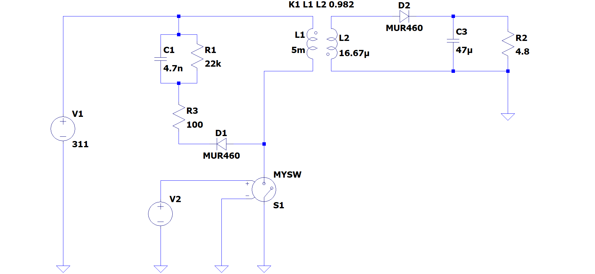
The circuit used can be seen below. The output is connected to GND so that the simulation can be calculated using numerical methods.
 Circuito simulado.
The following figure shows the transformer currents. In the real case, an oscillation can be notices during the switch OFF period caused by the resonances with the snubber circuit. During the ON period, a higher frequency oscillation is observed, which in this case is due to resonance with the parasitic capacitance of the output diode. By replacing the output diode with an ideal one, the higher frequency oscillations disappear.
![]() Transformer current simulation.
Transformer current simulation.
The following Figures show the output voltage, which stabilizes at a value below $12 V$ in both cases. For the ideal transformer, the difference with the target voltage is due to the output diode voltage drop, while in the real case higher losses appear due to leakage inductance and snubber circuit losses. According to the circuit design, this will be compensated through the feedback loop, increasing the effective duty-cycle and establishing $12 V$ at the output. On the other hand, an overshoot of approximately $15 V$ is noticeable at the start, which must also be compensated through the control carried out by the TinySwitch-4.
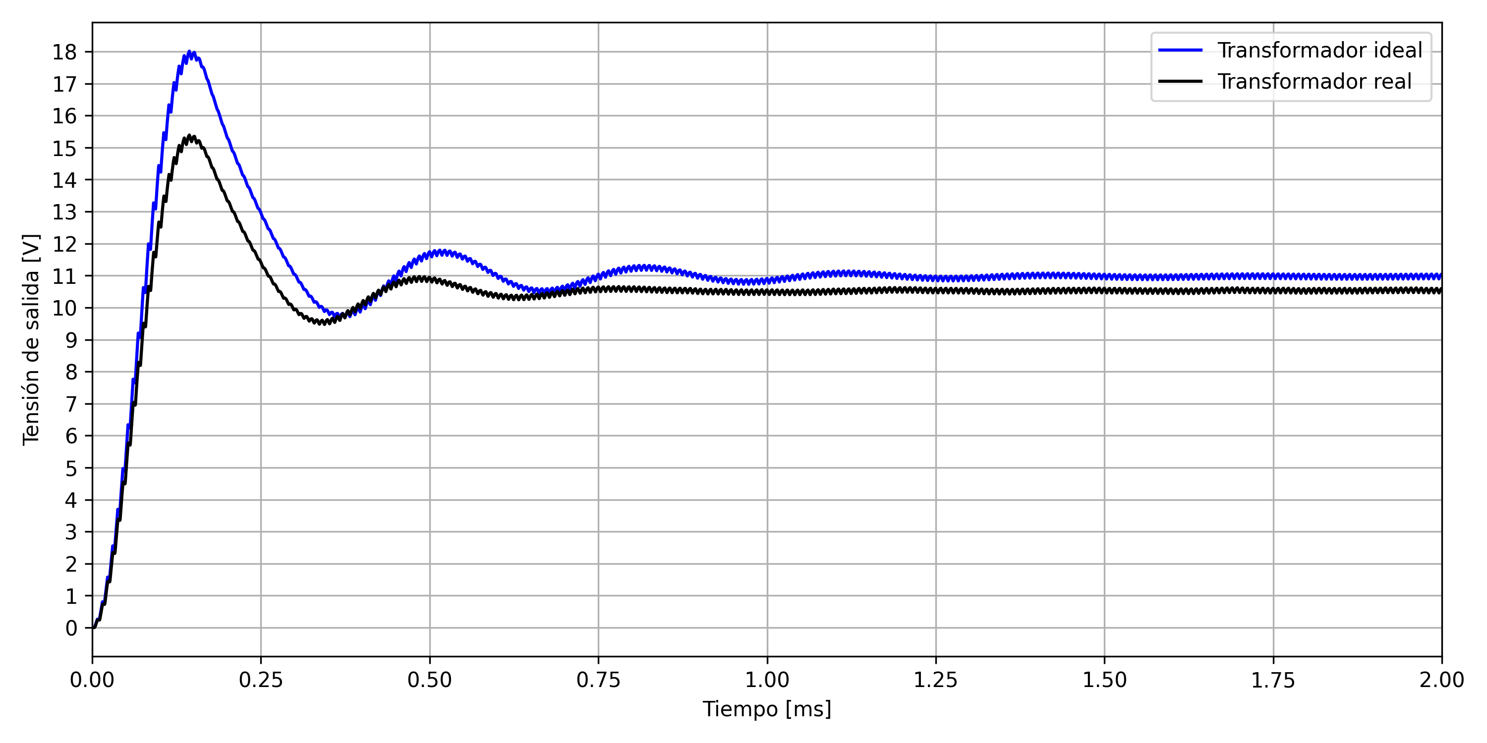 Output voltage simulation.
 Output voltage simulation.
The following Figures show the voltage on the switch, which according to the limitations of the TNY290PG should never exceed $725 V$. In both cases, the steady state voltage value coincides with the results presented in the previous section, below the mentioned limit. However, an overshoot occurs at startup which has the potential to damage the integrated circuit. This should not be a problem in the real implementation since, as mentioned, the control that the TinySwitch-4 performs on the output voltage prevents the appearance of such a high voltage at the input.
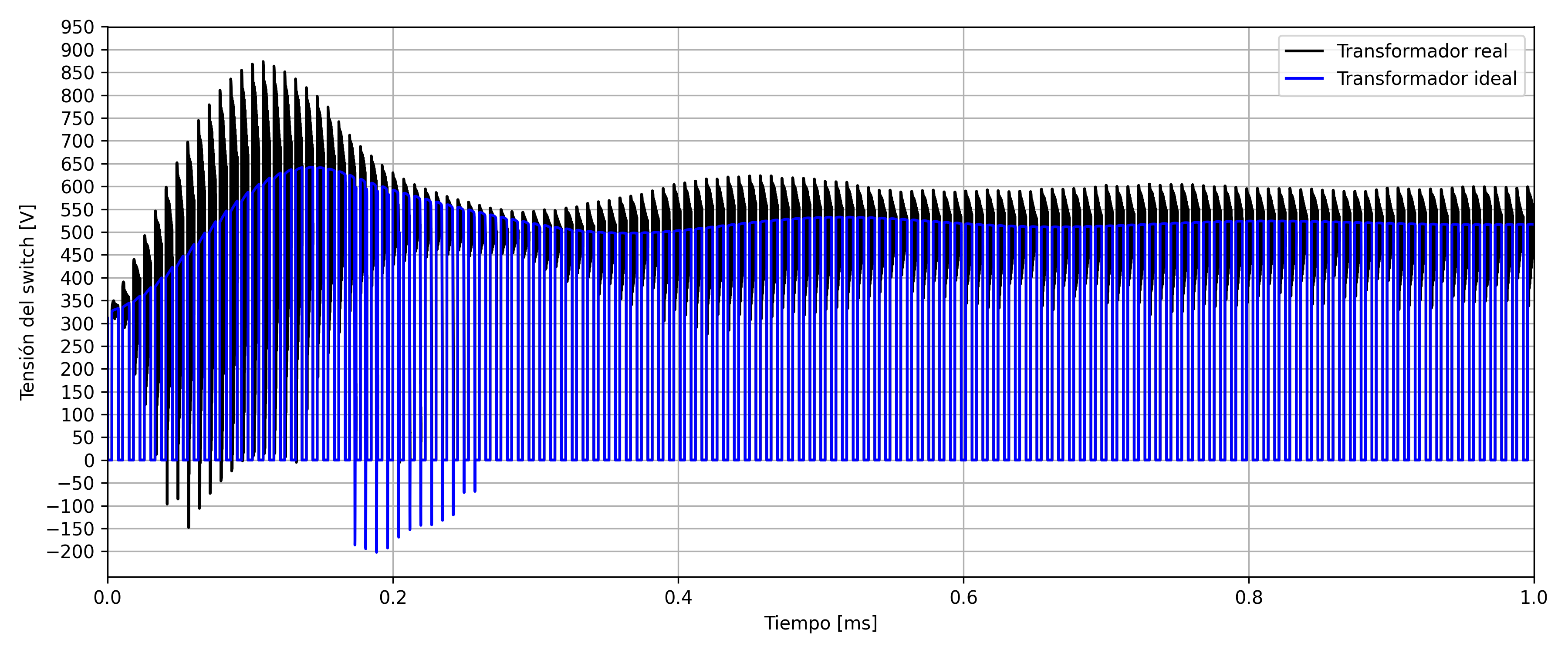 Switch voltage simulation.
 Switch voltage simulation.
The following Figure shows the currents present in the snubber circuit. The initial current peak caused by the leakage inductance can be noticed. Moreover, the same oscillations are observed as in the primary current due to the resonance between these elements. Finally, a very pronounced negative peak is observed which can be attributed to the recovery current of the snubber circuit diode, which in the real implementation will be much less pronounced because of all the parasitic resistances and capacitances that limit the peak value of this current. Additionally, it can be verified that the snubber resistor dissipates an approximately constant power of $3.2 W$. This reflects the leakage inductance value, which is very high, and could be decreased by replacing the hand-winded tranformer with a properly manufactured one.
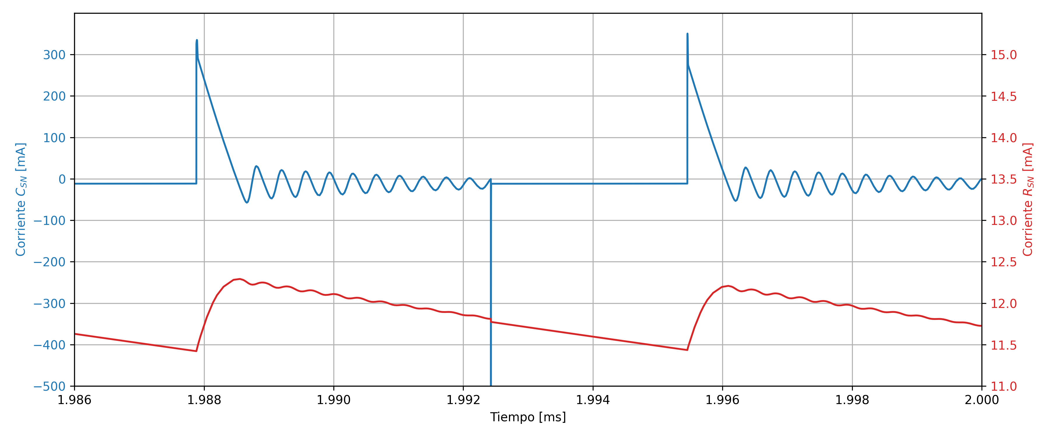 Simulation of the currents in the snubber.
Transformer measurements 🔗
Once the transformer was wound, it was measured using the laboratory’s LCR meter. To verify the inductance of the primary and secondary winding, the opposite winding is left as an open-circuit while the secondary is short-circuited to measure the leakage inductance of the primary. In the following Figure you can see a photograph of the measurement of the secondary winding; the measured value corresponds approximately to the calculated theoretical value of the inductance $L_2$, as seen in the design results table.
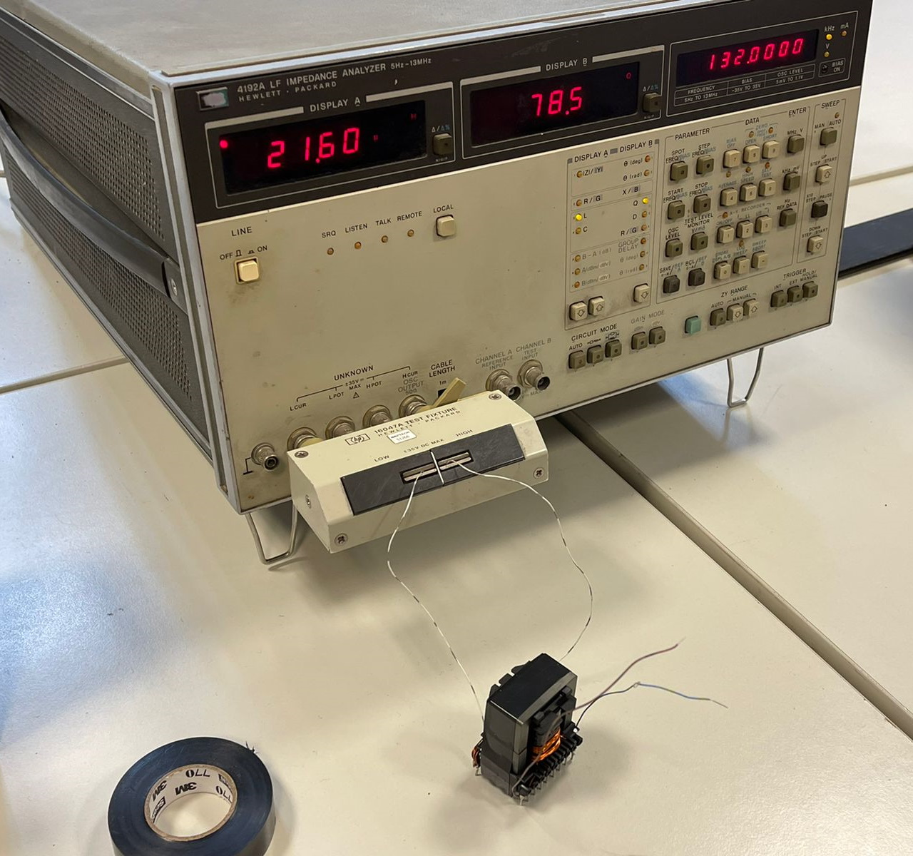
Additionally, the relationship $N_1/N_2$ was verified by applying a sinusoidal signal with a functino generator to one of the windings, and measuring the output signal in the other winding with an oscilloscope.
Circuit Measurements 🔗
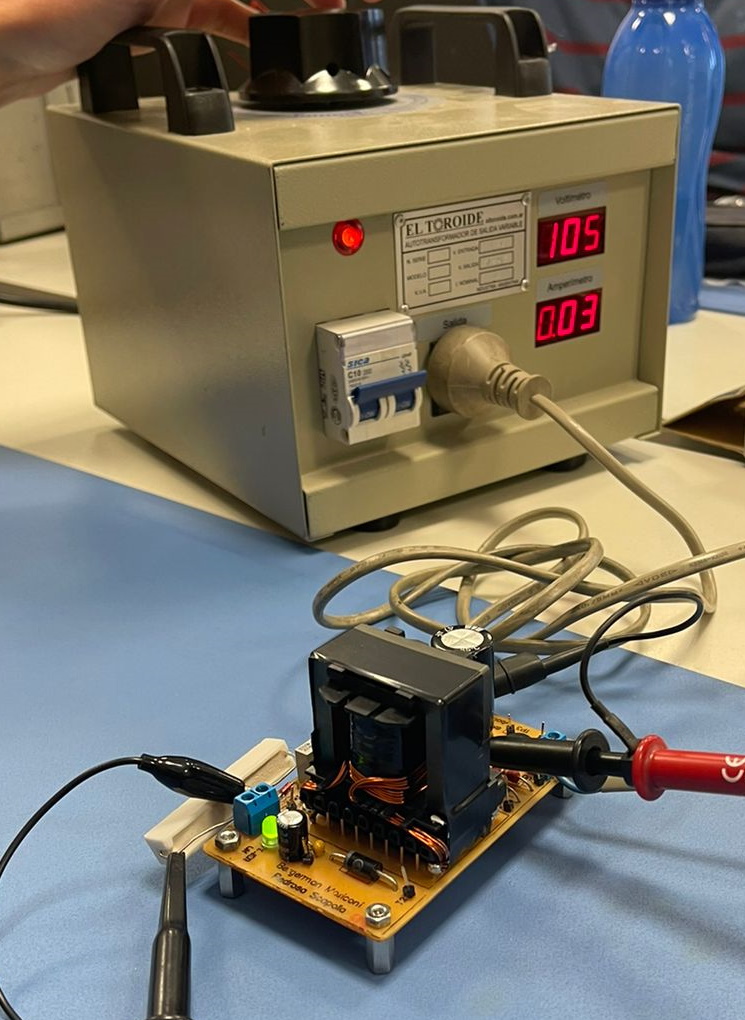
The measurements were made using an autotransformer (Variac) galvanically isolated from the line voltage to protect the oscilloscope. The load connected for the measurements was such that the output power is approximately $20W$, when changing the load to obtain a power of $30W$, analogous results were observed. The voltage of the autotransformer was gradually increased until reaching the final value of $220V$ for each measurement made. In the following Figure a photograph can be seen of the circuits power connections.
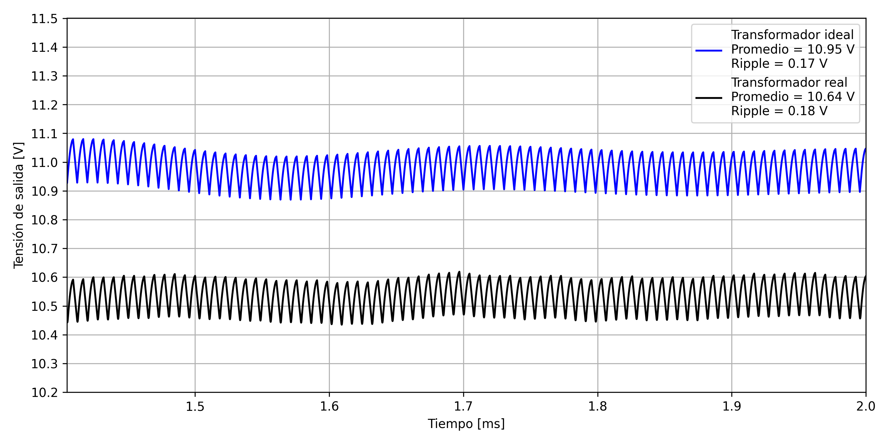
The following Figure shows the output voltage, it has an average value of $12V$ thanks to the calibration carried out through the variable resistor and the control carried out by the TinySwitch-4. The voltage presents a higher ripple than expected, of approximately $1.8 V$. This phenomenon is attributed to the peak recovery current of the output diode, as well as in part to the ESR of the output capacitor.
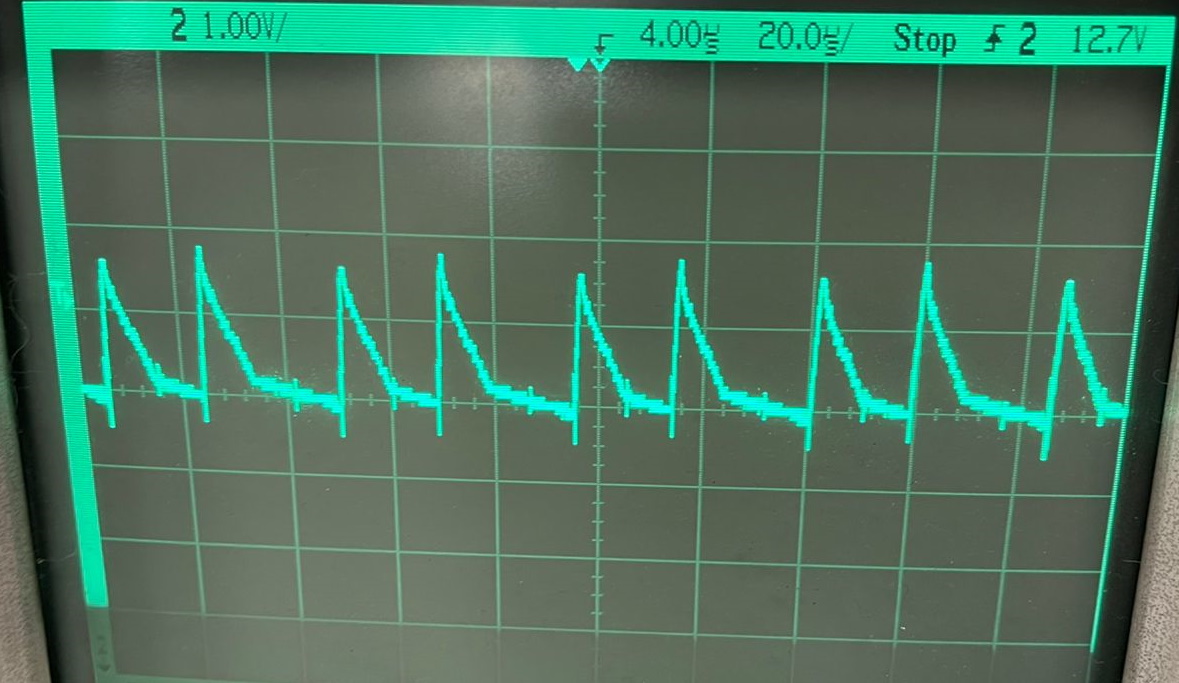 Output voltage measurements.
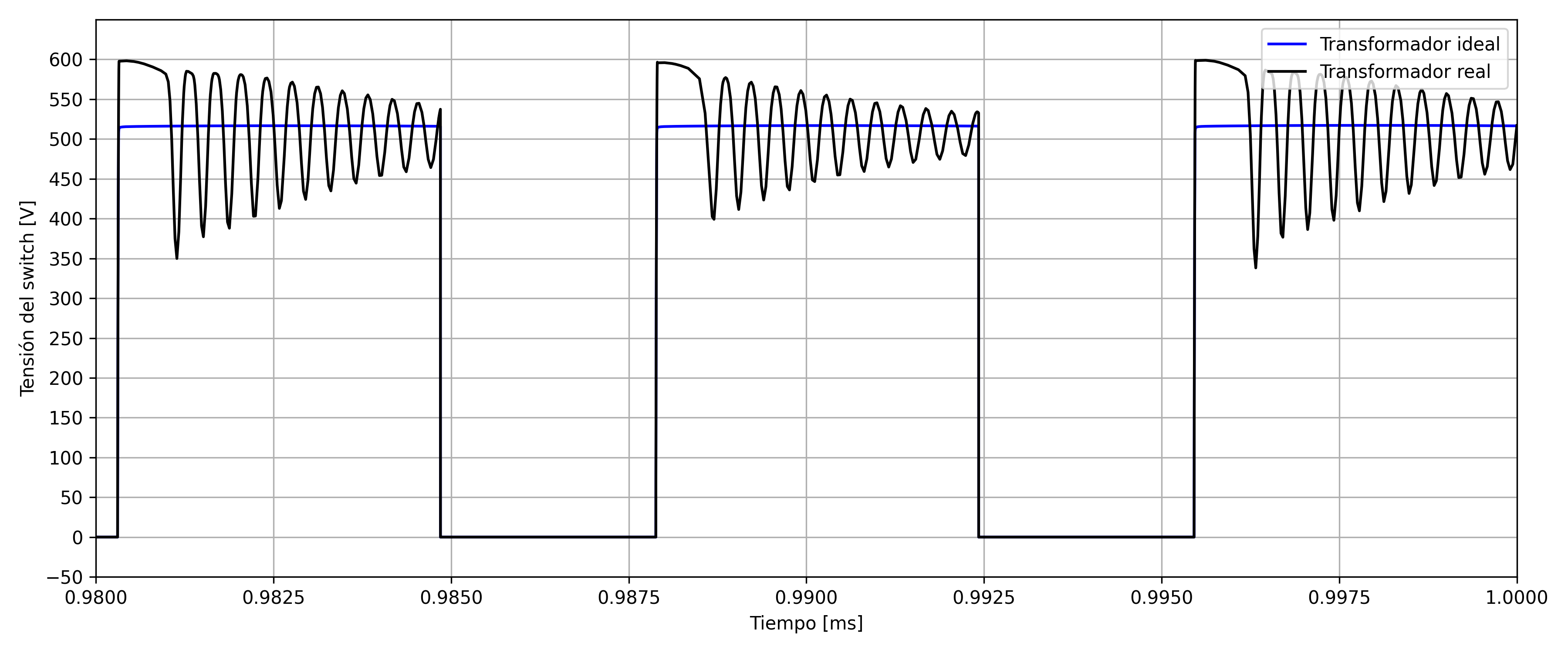
The following Figures show the voltage over the Drain of the MOSFET:
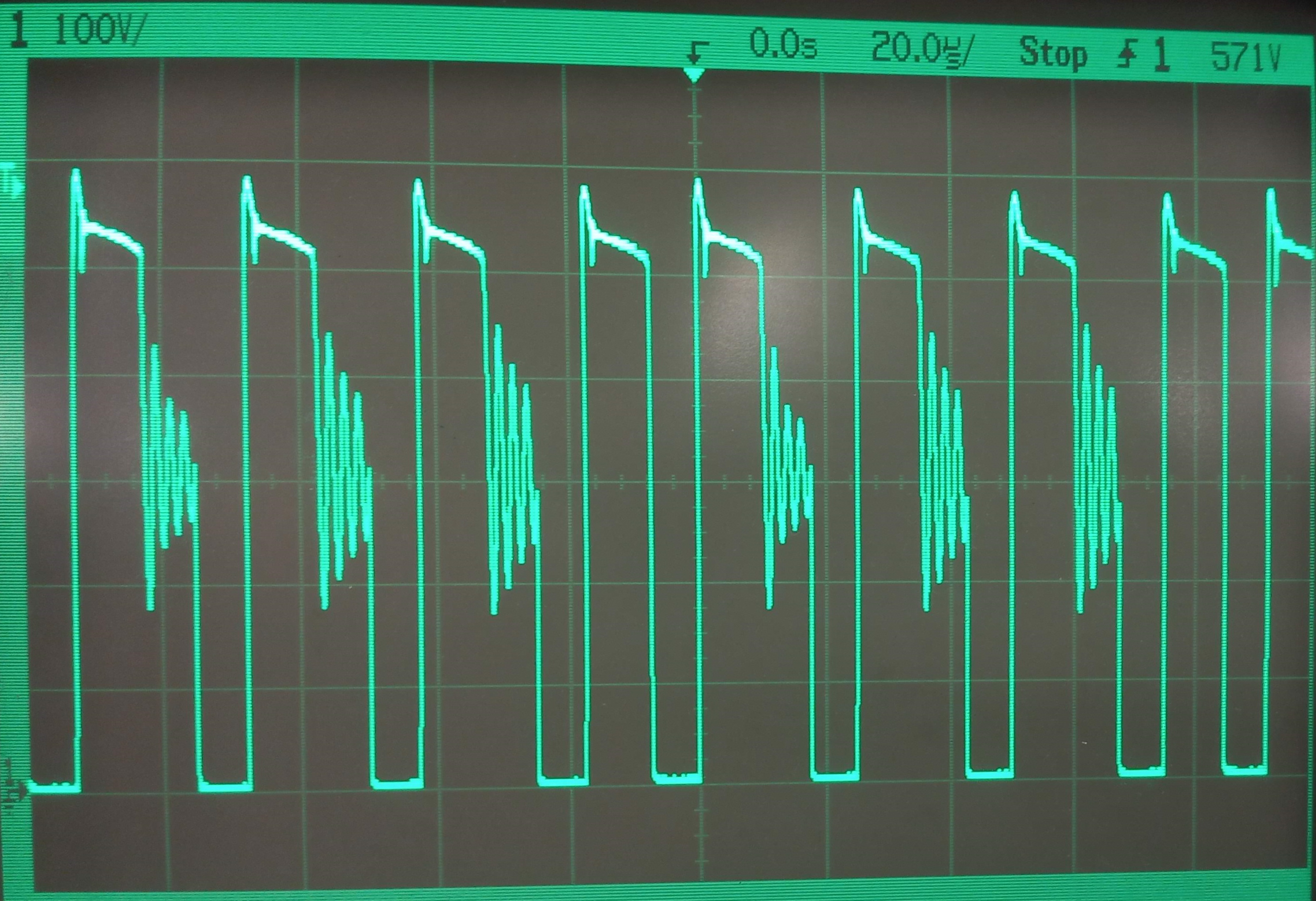
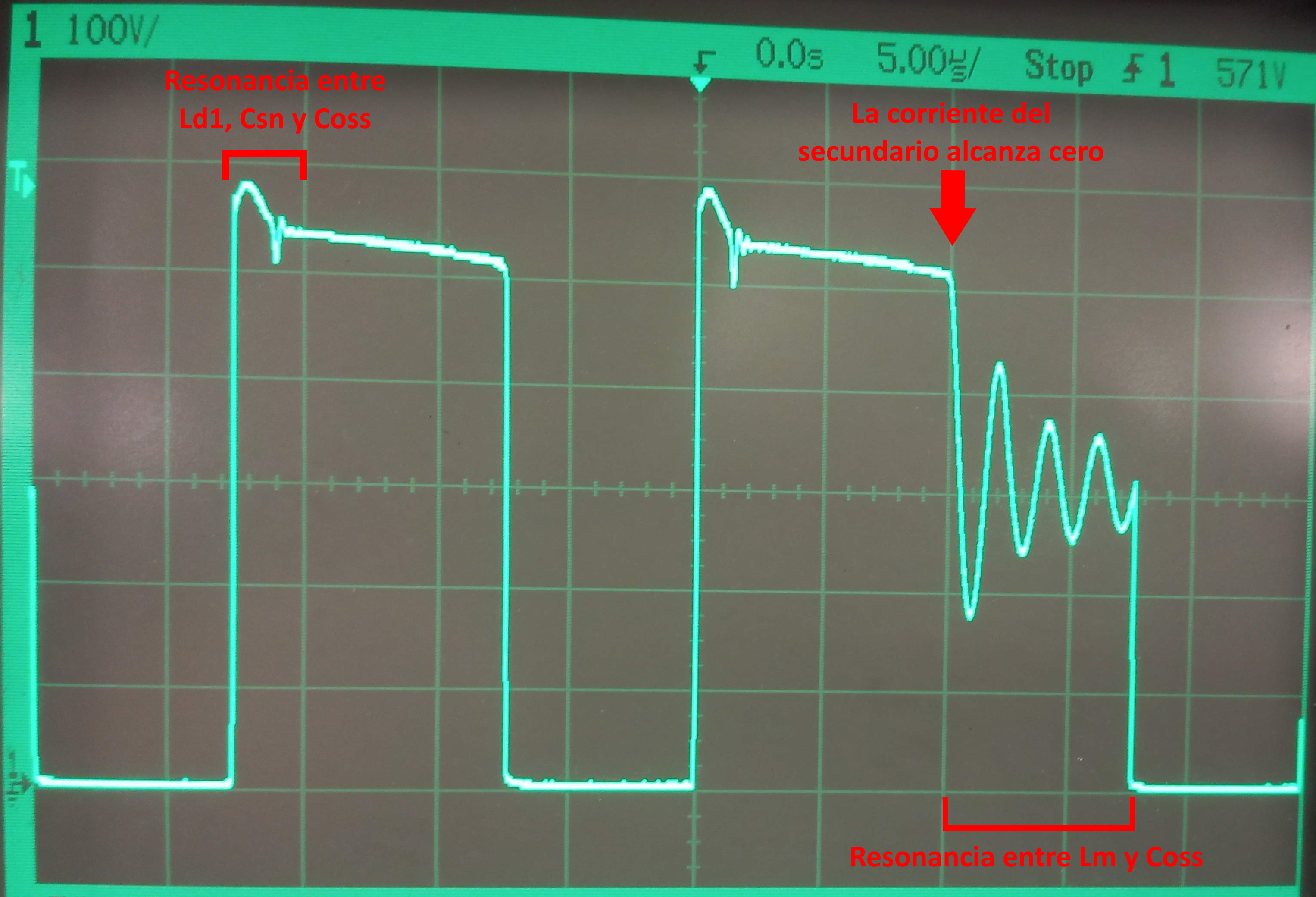
These images show the voltage peak at the moment of shutdown that is attenuated by the snubber circuit, always staying below $600V$. However, it is noted that the resonances present in the simulation have a lower amplitude on the circuit measurements, since these are attenuated by the losses present on the board and the real components. Additionally, it can be seen that the dynamic current limit established by the TinySwitch-4 is such that in certain cycles the system operates in discontinuous mode while in others it operates in continuous mode. This phenomenon is evidenced in the appearance of oscillations during the shutdown time, due to the fact that when the secondary current reaches zero, a recovery current appears in the output diode that excites the resonating circuit formed between the magnetizing inductance of the transformer and the capacitances of the MOSFET. When modifying the load, it was observed that the percentage of cycles in DCM decreases as the load increases, reaching almost all the cycles in CCM for $P_o=30W$.