FPGA-controlled Inverter design
2022 / Matías Bergerman, Franco Moriconi, Carola Pedrosa, Franco Scapolla
Project overview 🔗
The goal of this project is to design an Inverter board in order to control a 125 W three-phase motor from the 220 V power line. This design uses IR2110 MOSFET drivers, and the modulation is performed with a stand-alone board called UPduino 3 which features a Lattice UltraPlus ICE40UP5K FPGA.
Inverter design 🔗
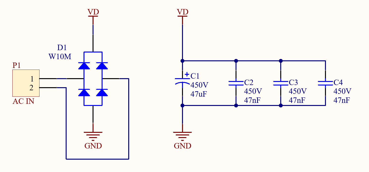
For the design of the Inverter board, IR2110 IC datasheet provides some considerations which are taken into account. The circuit input is a line voltage of $220 V_{rms}$, which passes through the laboratory variac, and is then rectified by a diode bridge (model W10M) that provides the DC voltage $V_{d}$ that connect to the of the Drain of the MOSFET in each of the three phases. In addition to the 47uF electrolytic capacitor that is part of the rectifier, a 47nF polyester capacitor was added between $V_d$ and $GND$ as close as possible to the MOSFETs of each of the three phases. This can be seen in the schematic below:
Then, DC power feeds each of the phases, as can be seen below:
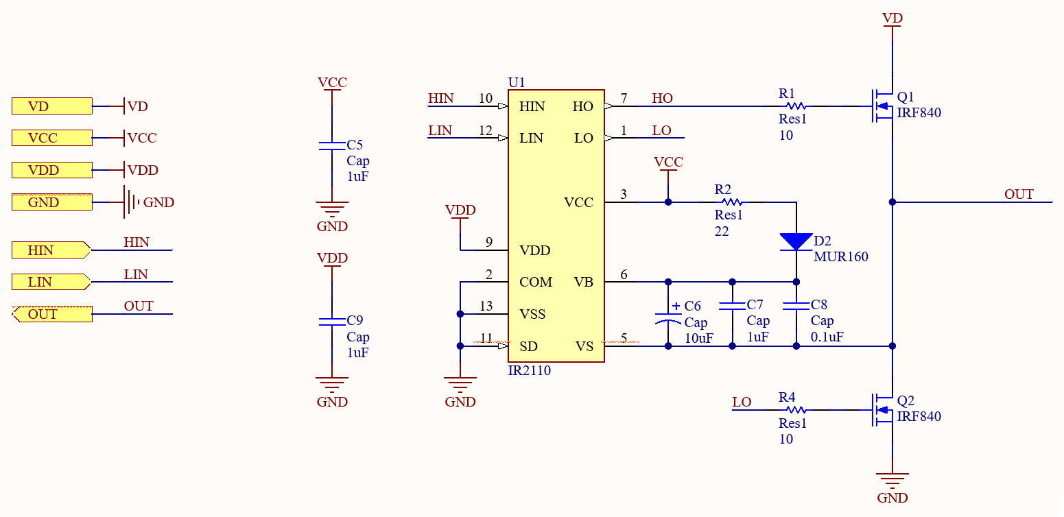
For this part, there are $2$ new power nets: $V_{CC}$ is the one that supplies the IR2110 with a voltage of $15 V$, and $V_{DD}$ is the digital supply voltage of $3.3V$ which is equivalent to the logic levels of the FPGA. Following the recommendations of the datasheet, the $COM$, $V_{SS}$ and $SD$ pins of the IC are connected to ground. The $HIN$ and $LIN$ signals are the digital output signals from the FPGA; The signals $HO$ and $LO$ are obtained at the output of the IR2110 IC, which effectively control the Gate voltage of the MOSFETs and are the ones in charge of carrying out the switching. It should be noted that a “dead time” is inserted by the FPGA in order to guarantee that one MOSFET always turns off before turning on the other, so that both are never on at the same time.
The objective of using this IC is to be able to supply the gate current required by the MOSFETs, as well as implement a bootstrap trigger circuit. To do this, based on the datasheet of the IC and the application notes provided by the manufacturer, the $D_2$ diode and the bootstrap capacitor formed by $C_6$ , $C_7$, and $C_8$ are added to the circuit. By combining capacitors of different technology (electrolytic and ceramic multilayer) it is possible to lower the equivalent ESR of the capacitors. A bootstrap resistor $R_2$ is also added, whose main function is to limit the current during power-up, since at the beginning of power-on the bootstrap capacitor is not charged. The idea behind this circuit is that during the turn-on time of transistor $Q_2$, the bootstrap capacitor charges through the diode with the voltage $V_{CC}$. This generates a voltage difference of $V_{CC}$ between $V_B$ and $V_S$. The way the IC works, when it is $Q_1$’s turn to switch on, the $HO$ output is connected to $V_B$. So the Gate voltage of $Q_1$ is approximately $V_B$ while the Drain voltage is $V_S$. Then, the voltage $V_{GS}$ of $Q_1$ will be $V_{CC}$, which, as mentioned above, is chosen to be greater than the threshold voltage of the MOSFET and effectively trigger it.
Circuit simulation 🔗
MATLAB simulations 🔗
To simulate the circuit MATLAB is used, as seen in the following image.
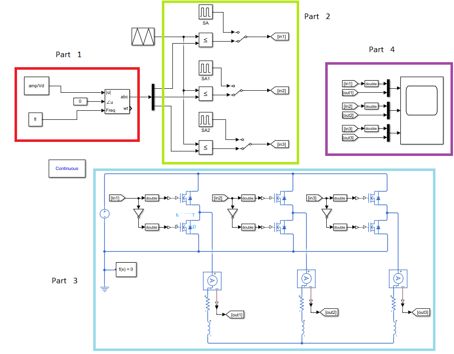
The circuit is divided into the following parts:
- Part 1: An external script
confg.mis used to configure the three-phase sinusoidal input to each of the inverter phases. - Part 2: A manual switch is used to choose between square modulation or sinusoidal modulation. In the case of sinusoidal modulation, the sine wave generated in Part 1 is compared with a triangular one of frequency $m_{f}\cdot f_{l}$, where $f_{l}$ is the frequency of the sine from Part 1. With this, we obtain the signal that switches the MOSFETS from the same branch on and off.
- Part 3: We have the 3 branches of the inverter (one for each phase) and the output is measured using an ammeter. It should be noted that a NOT gate is added between the MOSFETS of the same branch so that both do not turn on simultaneously. An inductive load is added to the circuit to simulate the motor which will be added to the actual circuit.
- Part 4: Finally, scopes are added to measure the input (signal that switches the MOSFETs of each branch on and off) and the output (current of each phase).
Then, the following signals are obtained at the output:
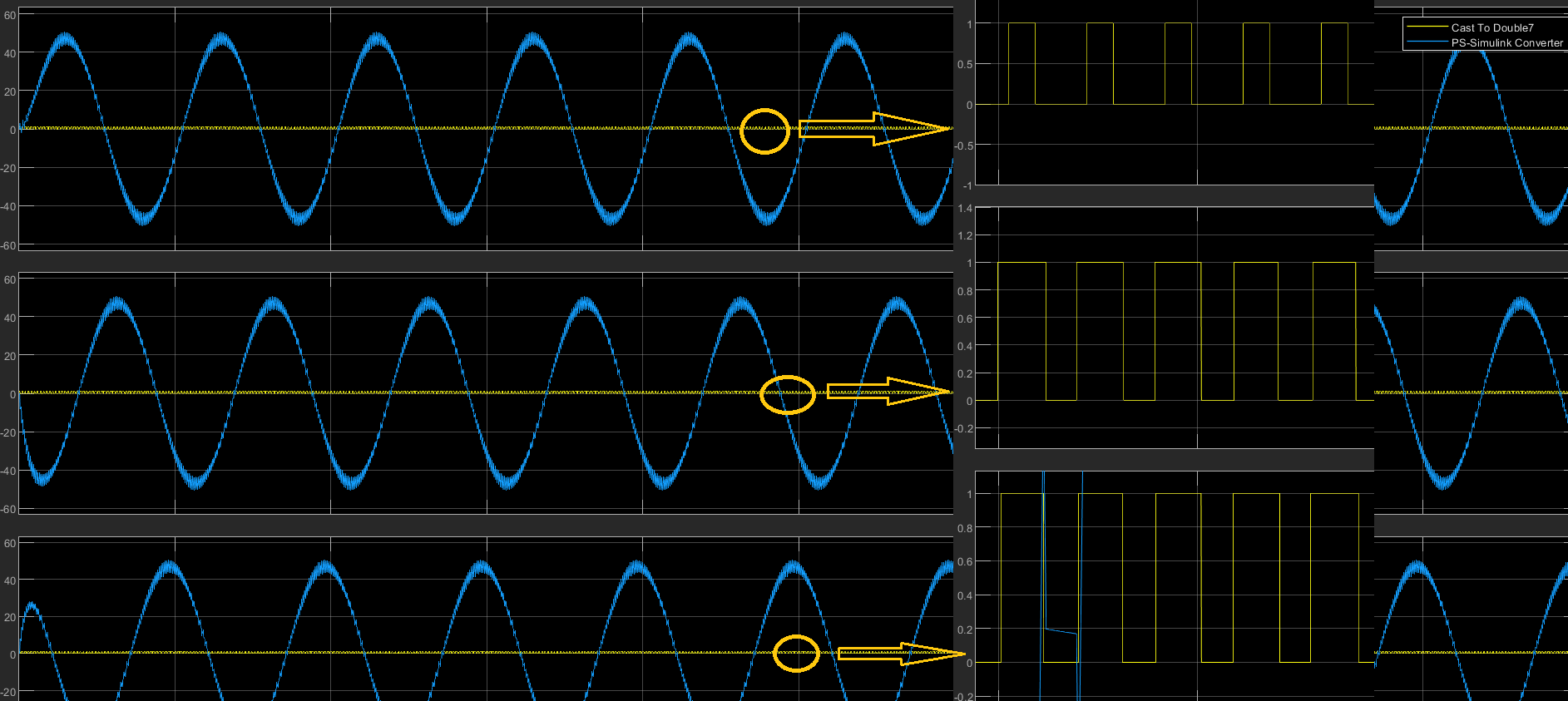
Where the 3 sinusoidal outputs are observed 120 degrees out of phase and the square signal that turns the MOSFETS of each branch on and off, as expected.
LTSpice simulations 🔗
The inverter is simulated in LTspice, as seen in the following image:
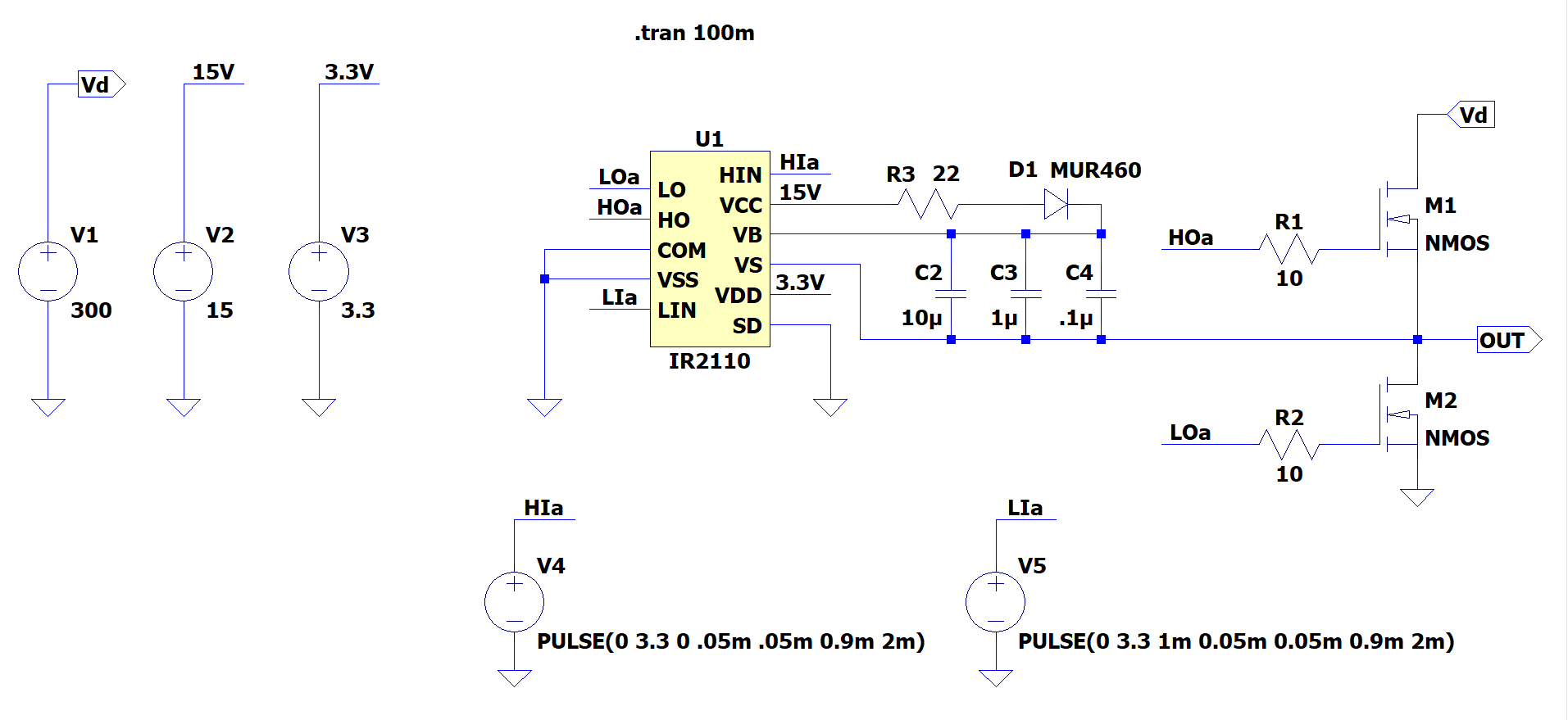
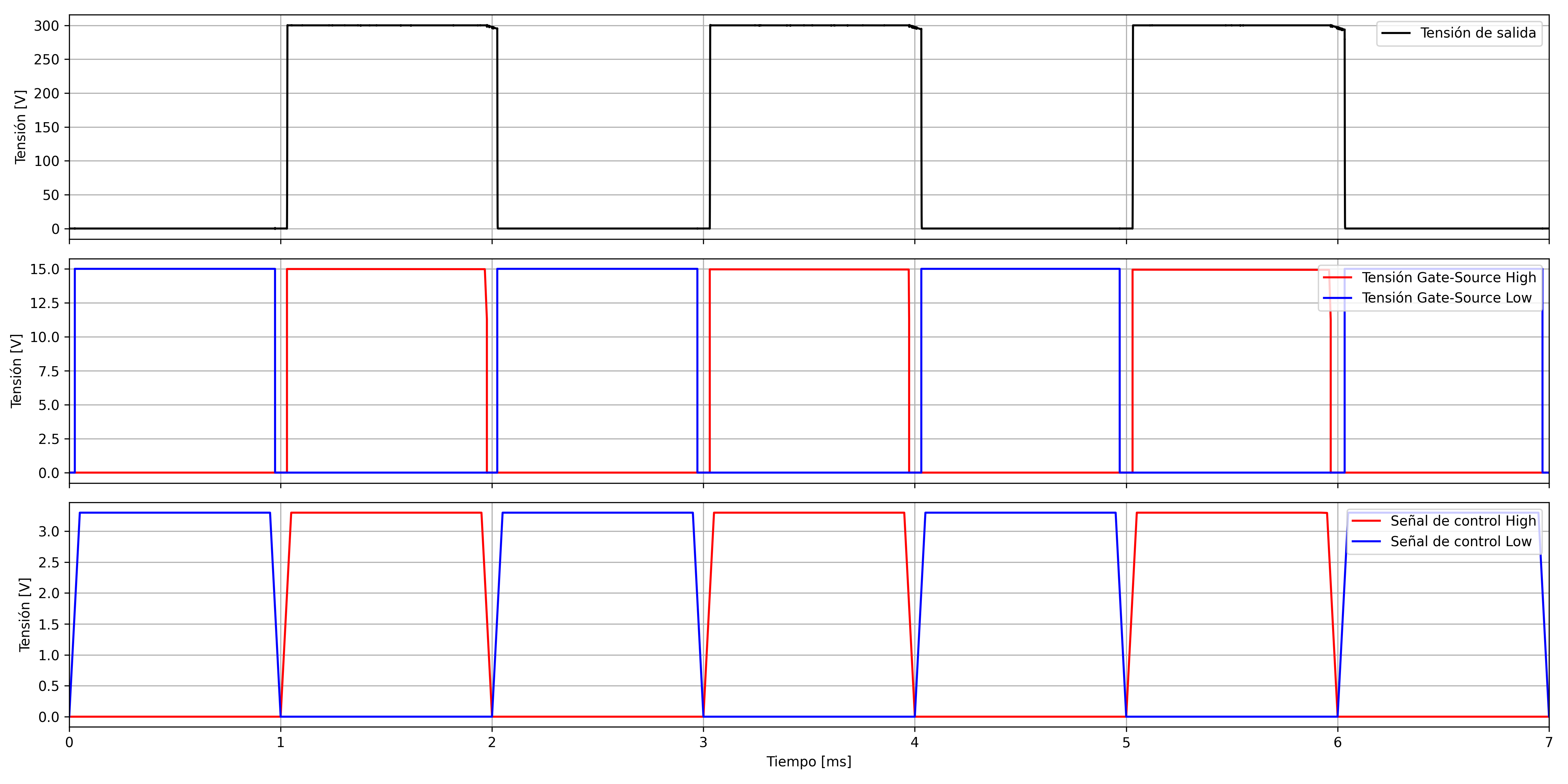
Using the Spice model provided by the manufacturer, the correct operation of the bootstrap triggering circuit was verified. The following figure shows the results of this simulation. As can be seen, in the steady state with the bootstrap capacitor charged, the voltage $V_{gs}$ of both transistors is higher than the threshold, since $HOa$ reaches approximately $315 V$ when the signal $HIa$ is turned on. Moreover, the schmidt trigger effect of IR2110 is evidenced.
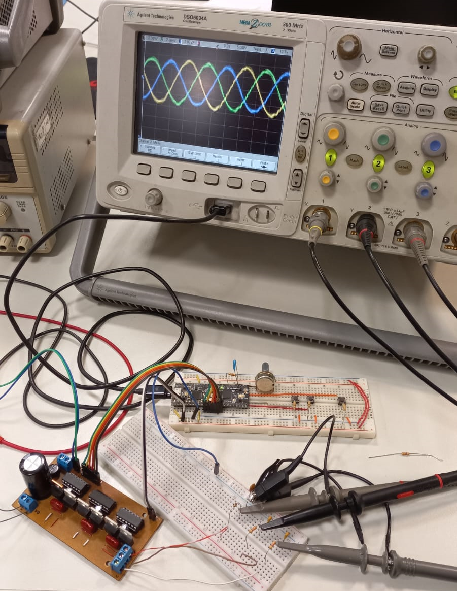
Inverter implementation 🔗
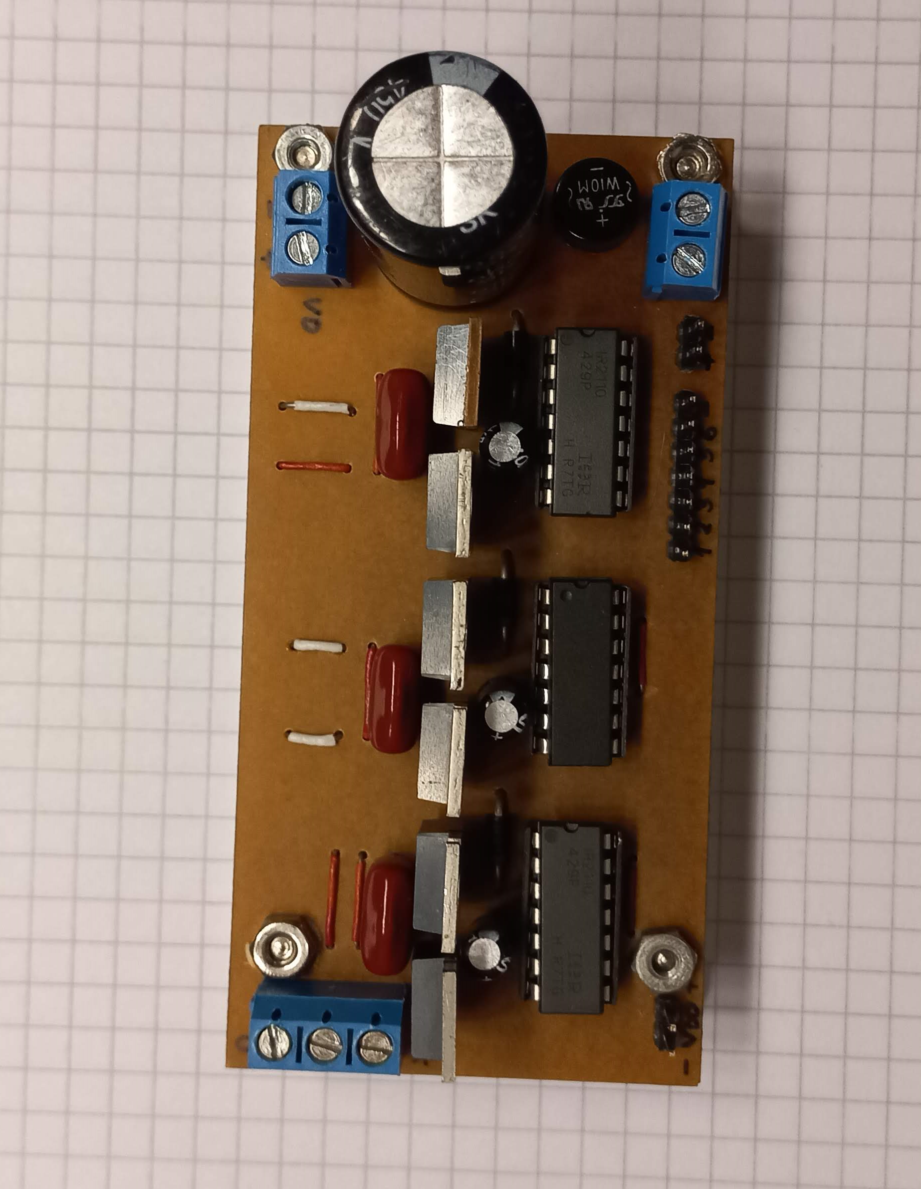
In the next figure the manufactured PCB design is shown, along with a photograph of the final system working which generates 3 sinusoidal signals offset by 120 degrees (these are obtained with the use of an RC low-pass filter of the digital signals).
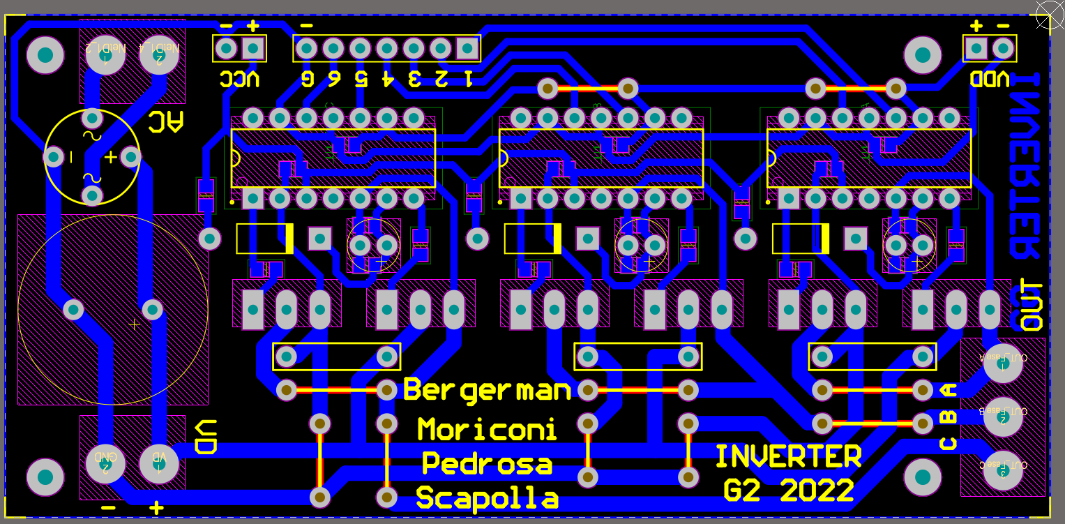
Printed circuit board 🔗
For the design of the PCB, various considerations were taken into account, such as the minimization of the inductance present in the Gate signals and the power supply connections of the power elements. Therefore, for these traces, soldered bridges were avoided, their length was reduced, and SMD components were used. Additionally, low-ESR bypass capacitors were added in close proximity to each power element, such as the MOSFETs and IR2110 ICs. The final size of the PCB is 5cm x 10cm.
V/f control 🔗
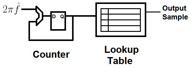
For the V/f control of the motor, a circuit was implemented with the UPduino 3 development board that has a Lattice UltraPlus ICE40UP5K FPGA. The three phases are generated by tables in memory, which are accessed using an NCO (Numerically-Controlled Oscillator) of which a diagram can be seen in a following figure. In this way, the frequency of the sine wave can be varied by modifying the constant that is added to the counter in each clock cycle. To achieve good precision and range in terms of available frequencies, fixed-point decimal numbers are used for both the counter value and the constant added to it at each clock cycle. Thus, the counter keeps track of all its decimal places but only the integer part is interpreted as the address of the lookup table.
The table samples are scaled by the desired amplitude and finally these are received by a PWM module that generates a signal with a duty cycle proportional to its input. This PWM module is also responsible for adding “dead-time” to prevent at all costs that two MOSFETs of the same phase are activated simultaneously.
V/f control is achieved by modifying the frequency and amplitude in conjunction, multiplying both by the same factor. In order to achieve a constant factor $m_f=51$, the period of the PWM module must also be modified in conjunction with the NCO. Since the period scales inversely proportional to the frequency, it is necessary to perform a division operation. In our case, adding a division to the HDL code causes an excessive use of the FPGA resources, exceeding the total amount present. To solve this problem, it was decided to carry out the division using a table in memory (lookup table), since the divisor changes but the dividend remains constant.
Lastly, the user interface was implemented using 2 push-buttons to increase or decrease the V/f constant in discrete steps and the on-board RGB led is used to display the current value of the V/f constant. For a given constant, the speed and frequency are gradually controlled together by using a potentiometer, the value of which is obtained with a sigma-delta ADC converter implemented on the same FPGA along with an external capacitor and resistor.